Navigate complex analog signal paths with confidence using ADG738 and STM32F405RG
Solving analog puzzles: The MUX is the key!
Published Oct 07, 2023
Click board™
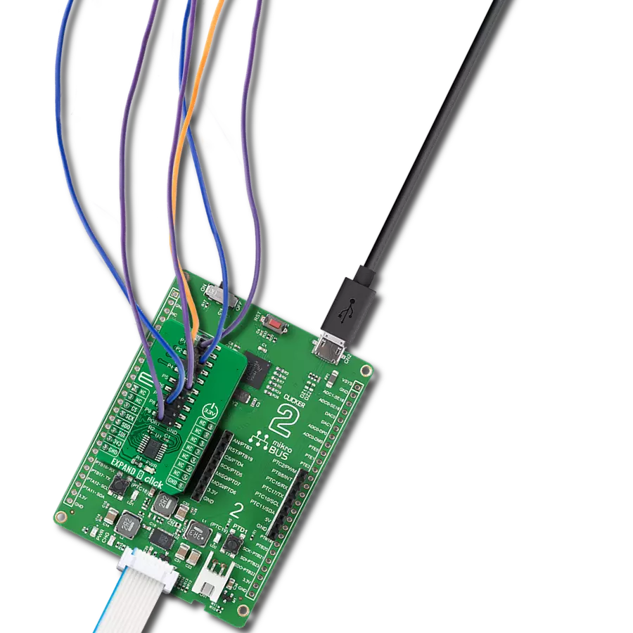
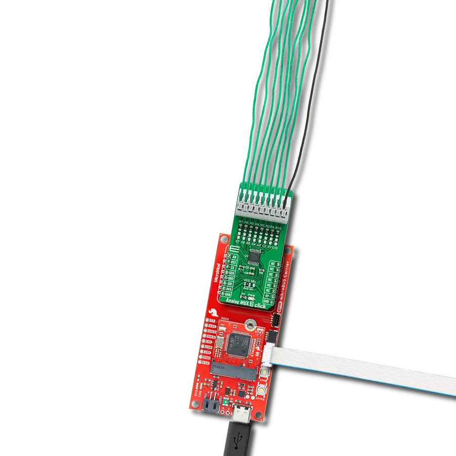
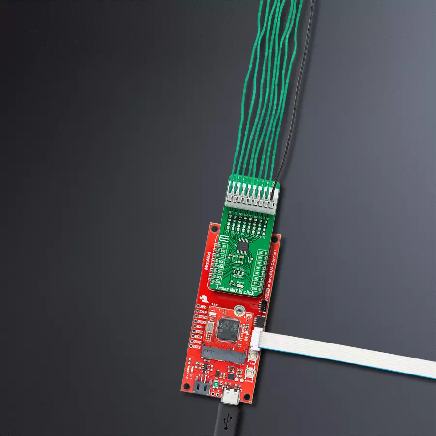
Analog MUX 3 Click
Dev. board
SparkFun MicroMod mikroBUS Carrier Board
Compiler
NECTO Studio
MCU
STM32F405RG
Empower industrial automation and control applications with our analog mux, facilitating efficient monitoring and control of various sensors and instruments
A
A
Hardware Overview
How does it work?
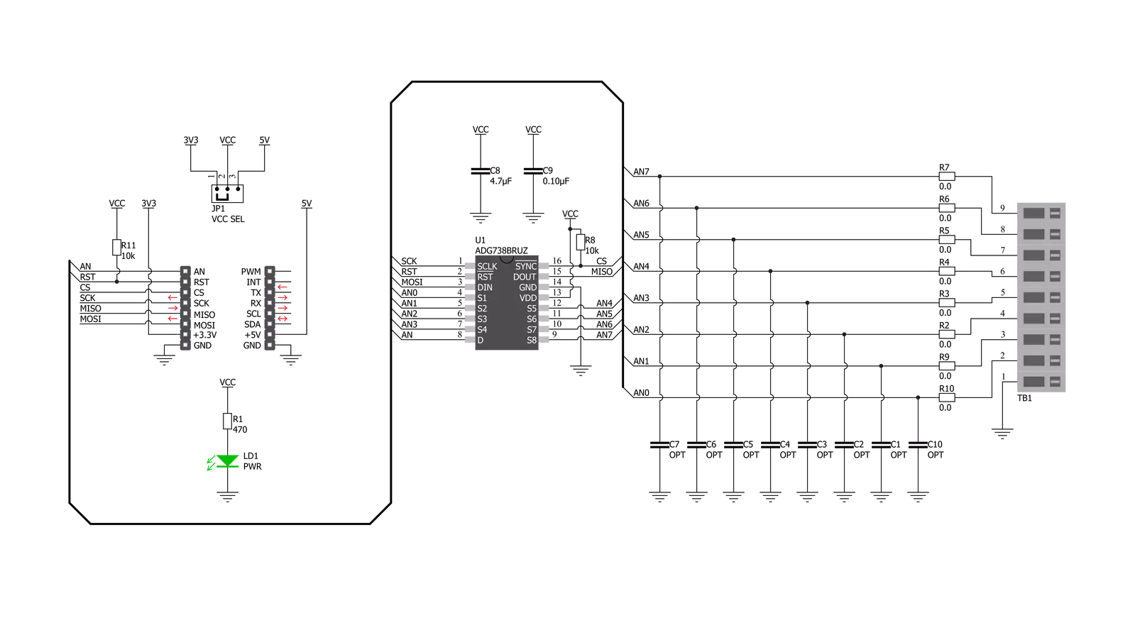
Analog MUX 3 Click is based on the ADG738, a CMOS 8-channel analog matrix switch with a serially-controlled SPI interface from Analog Devices. The ADG738 can operate equally well as a multiplexer, demultiplexer, or switch array, providing more flexibility. It also features a low on-resistance closely matched between switches and flat over the entire signal range. During the Power-Up of the ADG738, all switching channels will be in the OFF condition, and the internal shift register will contain all zeros and remain so until a valid write takes place. All channels exhibit 'break-before-make switching action, preventing momentary shorting when switching channels. Each bit of the 8-bit serial word corresponds to one device switch. Internal switching channels are independently controlled by an individual bit,
providing an option to activate any, all, or none of the switches. All of the input channels of the multiplexer can be easily connected to a nine-pole spring action block terminal without having to use any additional tools, such as screwdrivers, while the output pin from the multiplexer is routed to the AN pin on the mikroBUS™ socket. A new 8-bit word is written to the input shift register when changing the switch conditions. Some of the bits may be the same as the previous write cycle, as the user may not wish to change the state of some switches. To minimize glitches in these switches' output, the ADG738 cleverly compares the state of switches from the previous write cycle. If the switch is already in the ON state and needs to stay in that condition, there will be minimal glitches in the switch's output. Analog MUX 3 Click
communicates with MCU using the SPI serial interface compatible with standard SPI, QSPI™, MICROWIRE™, and DSP interface standards and operates at clock rates up to 30MHz. Also, this Click board™ has a Reset pin routed to the RST pin on the mikroBUS™ socket, which clears the input register and turns all switches to the OFF condition. This Click board™ can operate with either 3.3V or 5V logic voltage levels selected via the VCC SEL jumper. This way, both 3.3V and 5V capable MCUs can use the communication lines properly. Also, this Click board™ comes equipped with a library containing easy-to-use functions and an example code that can be used as a reference for further development.


Features overview
Development board
SparkFun MicroMod mikroBUS Carrier board takes advantage of the MicroMod, Qwiic, and mikroBUS™ ecosystems making it easy to prototype with each combined rapidly. The MicroMod M.2 socket and mikroBUS™ 8-pin header allow users to experiment with any processor board in the MicroMod ecosystem and any Click board™ in the mikroBUS™ ecosystem,
respectively. This board also features two Qwiic connectors to seamlessly integrate hundreds of Qwiic sensors and accessories into your project. The mikroBUS™ socket comprises a pair of 8-pin female headers with a standardized pin configuration. The pins consist of three groups of communications pins (SPI, UART, and I2C), six additional pins (PWM, Interrupt, Analog input,
Reset, and Chip select), and two power groups (3.3V and 5V). While a modern USB-C connector makes programming easy, the Carrier Board is also equipped with an MCP73831 single-cell Lithium-Ion/Lithium-Polymer charge IC so you can charge an attached single-cell Li-Po battery. The charge IC receives power from the USB connection and can source up to 450mA to charge an attached battery.

Microcontroller Overview
MCU Card / MCU

Architecture
ARM Cortex-M4
MCU Memory (KB)
1024
Silicon Vendor
STMicroelectronics
Pin count
64
RAM (Bytes)
196608
Used MCU Pins
mikroBUS™ mapper
Take a closer look
Click board™ Schematic
Step by step
Project assembly

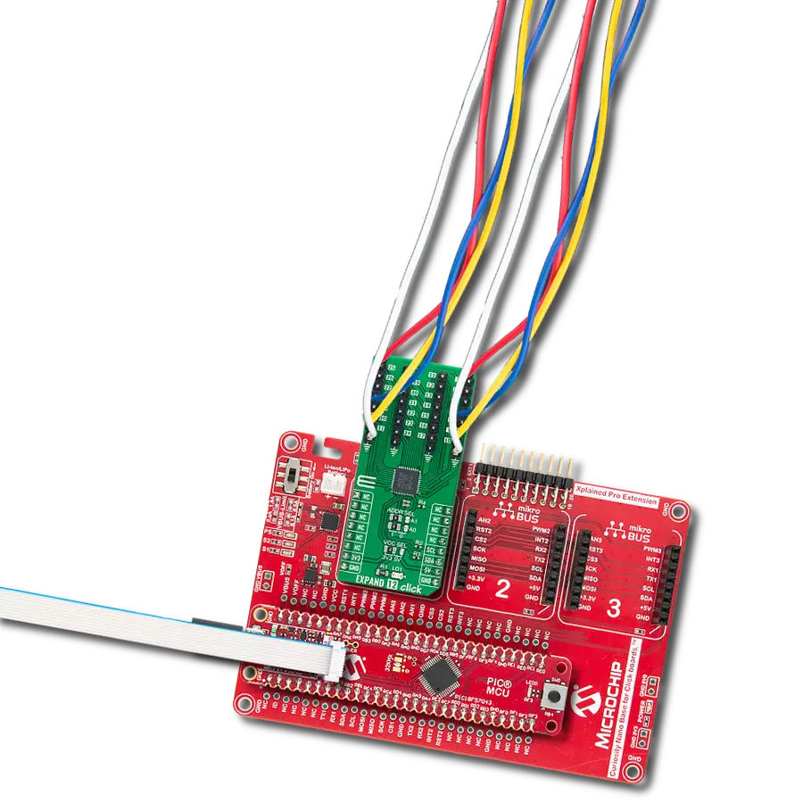
Start by selecting your development board and Click board™. Begin with the SparkFun MicroMod mikroBUS Carrier Board as your development board.


Software Support
Library Description
This library contains API for Analog MUX 3 Click driver.
Key functions:
analogmux3_generic_write- Analog MUX 3 data writing functionanalogmux3_set_channel- Analog MUX 3 set channel functionanalogmux3_read_an_pin_voltage- Analog MUX 3 read AN pin voltage level function
Open Source
Code example
The complete application code and a ready-to-use project are available through the NECTO Studio Package Manager for direct installation in the NECTO Studio. The application code can also be found on the MIKROE GitHub account.
/*!
 * @file main.c
 * @brief AnalogMux3 Click example
 *
 * # Description
 * This is an example that demonstrates the use of the Analog MUX 3 Click board.
 * This application controls the multiplexing of a single input channel
 * with an eight-channel matrix switch.
 *
 * The demo application is composed of two sections :
 *
 * ## Application Init
 * Initializes SPI and ADC driver, set Vref, STM32F407ZG - 2.048 V, PIC18F97J94 3.3 V,
 * set the default configuration and start to write log.
 *
 * ## Application Task
 * This is an example that shows the use of a Analog MUX 3 Click board.
 * In this example, we switch from channel AN0 to channel AN7,
 * read and display the analog value and voltage on the active channel.
 * Results are being sent to the Usart Terminal where you can track their changes.
 *
 * @author Nenad Filipovic
 *
 */

#include "board.h"
#include "log.h"
#include "analogmux3.h"

static analogmux3_t analogmux3;
static log_t logger;

uint8_t read_data;

uint8_t read_byte;

void application_init ( void ) {
    log_cfg_t log_cfg;                /**< Logger config object. */
    analogmux3_cfg_t analogmux3_cfg;  /**< Click config object. */

    /**
     * Logger initialization.
     * Default baud rate: 115200
     * Default log level: LOG_LEVEL_DEBUG
     * @note If USB_UART_RX and USB_UART_TX
     * are defined as HAL_PIN_NC, you will
     * need to define them manually for log to work.
     * See @b LOG_MAP_USB_UART macro definition for detailed explanation.
     */
    LOG_MAP_USB_UART( log_cfg );
    log_init( &logger, &log_cfg );
    log_info( &logger, " Application Init " );

    // Click initialization.

    analogmux3_cfg_setup( &analogmux3_cfg );
    ANALOGMUX3_MAP_MIKROBUS( analogmux3_cfg, MIKROBUS_1 );

    // Vref STM32F407ZG
    analogmux3_cfg.vref = 2.048;

    // Vref PIC18F97J94
    // analogmux3_cfg.vref = 3.3;

    err_t init_flag  = analogmux3_init( &analogmux3, &analogmux3_cfg );
    if ( init_flag == SPI_MASTER_ERROR ) {
        log_error( &logger, " Application Init Error. " );
        log_info( &logger, " Please, run program again... " );

        for ( ; ; );
    }

    analogmux3_default_cfg ( &analogmux3 );
    log_info( &logger, " Application Task " );
    Delay_ms ( 100 );
}

void application_task ( void ) {
    for ( uint8_t ch_pos = ANALOGMUX3_SET_CHANNEL_0; ch_pos <= ANALOGMUX3_SET_CHANNEL_7; ch_pos++ ) {
        analogmux3_set_channel( &analogmux3, ch_pos );
        Delay_ms ( 1000 );

        uint16_t analogmux3_an_value = 0;

        log_printf( &logger, "   CHANNEL    : AN%u     \r\n", ch_pos );
        log_printf( &logger, "- - - - - - - - - - - - - \r\n" );

        if ( analogmux3_read_an_pin_value ( &analogmux3, &analogmux3_an_value ) != ADC_ERROR ) {
            log_printf( &logger, "   ADC Value  : %u\r\n", analogmux3_an_value );
        }

        float analogmux3_an_voltage = 0;

        if ( analogmux3_read_an_pin_voltage ( &analogmux3, &analogmux3_an_voltage ) != ADC_ERROR ) {
            log_printf( &logger, "   AN Voltage : %.3f V \r\n", analogmux3_an_voltage );
        }

        log_printf( &logger, "-------------------------\r\n" );
    }
}

int main ( void )
{
    /* Do not remove this line or clock might not be set correctly. */
    #ifdef PREINIT_SUPPORTED
    preinit();
    #endif

    application_init( );

    for ( ; ; )
    {
        application_task( );
    }

    return 0;
}

// ------------------------------------------------------------------------ END
Additional Support
Resources
Category:Port expander