使用GD5F2GQ5UEYIGR和STM32L496AG为任何应用添加数据存储
提升您的存储能力
已发布 7月 22, 2025
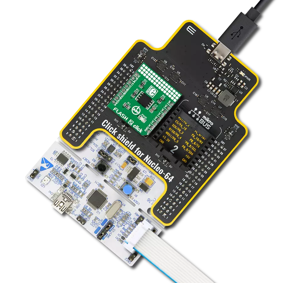
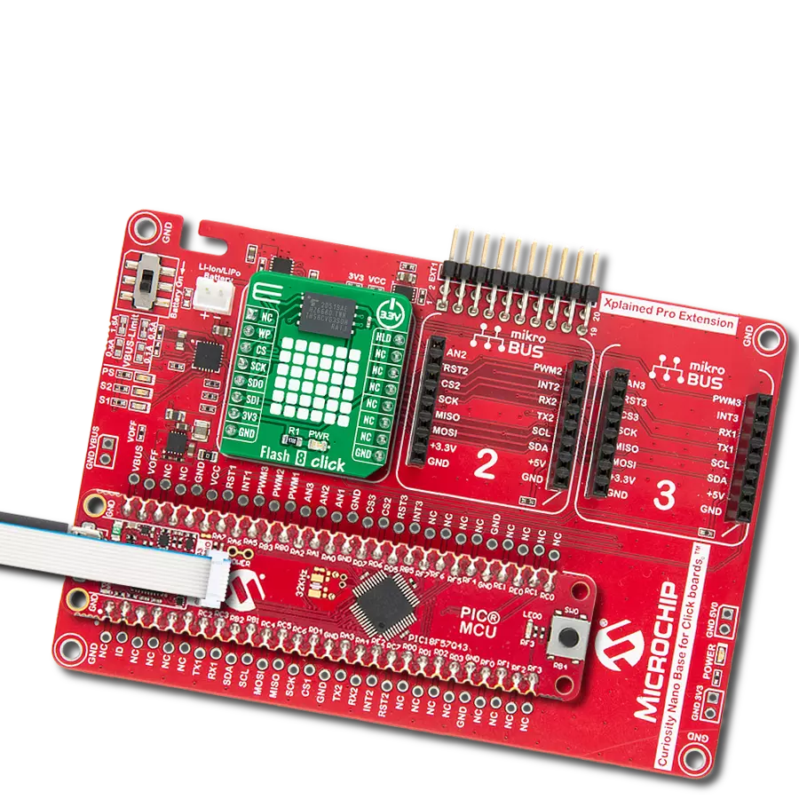
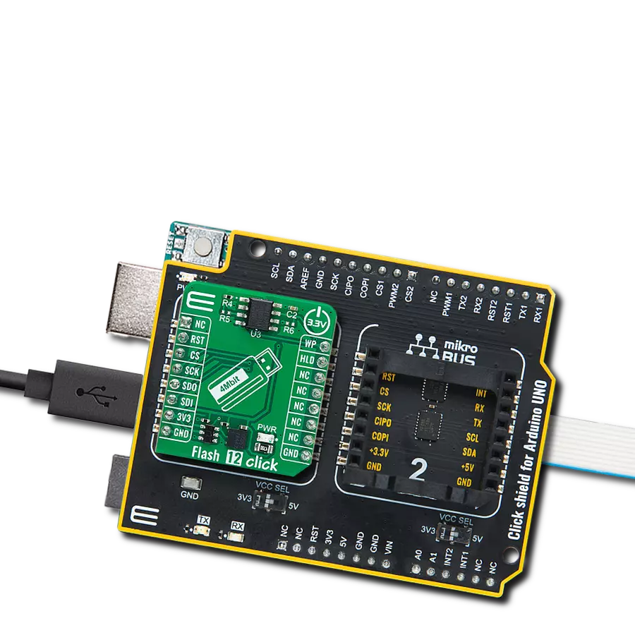
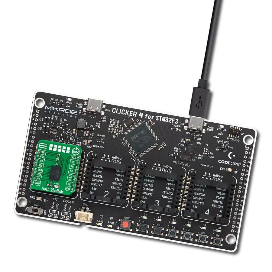
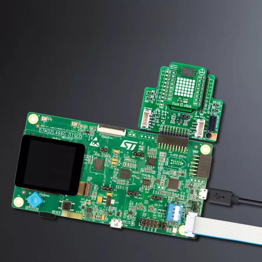
点击板
Flash 8 Click
开发板
Discovery kit with STM32L496AG MCU
编译器
NECTO Studio
微控制器单元
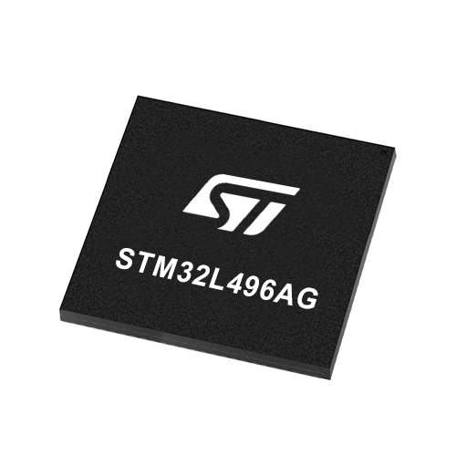
STM32L496AG
高可靠性存储解决方案
A
A
硬件概览
它是如何工作的?
Flash 8 Click 基于 GigaDevice Semiconductor 的 GD5F2GQ5UEYIGR,这是一种高度可靠的串行闪存解决方案,提供灵活性,设计用于各种消费应用。它具有 2Gb 的密度,基于行业标准的 NAND 闪存核心,代表了 SPI-NOR 和标准并行 NAND 闪存的具有吸引力的替代方案,并具有高级功能。GD5F2GQ5UEYIGR 组织为 256Mx8,具有先进的安全功能(8K 字节 OTP 区域)。它指定至少 100,000 次耐久周期,数据保留至少 10 年,使其能够处理对内存的无限次读取/写入。该 Click board™ 通过行业标准 SPI 接口(兼容 Dual 和 QSPI)与
MCU 通信,支持高时钟速度,支持两种最常见的 SPI 模式,SPI 模式 0 和 3,最大频率为 104MHz。它以基于页面的操作进行编程/读取,并以基于块的操作进行擦除。数据按页面传输到/从 NAND 闪存阵列,传输到数据寄存器和缓存寄存器,这些寄存器靠近 I/O 控制电路,充当 I/O 数据的数据缓冲区(启用页面和随机数据读取/写入和复制操作)。除了 SPI 通信外,该 Click board™ 还有两个额外的引脚用于写保护和 HOLD 功能,这些引脚连接到 mikroBUS™ 插座的 RST 和 PWM 引脚。可配置的写保护(标记为 WP 并连接到 mikroBUS™ 插座的 RST 引脚)防
止覆盖块锁定位,必须保持低电平以禁止所有对寄存器的写入操作。当该引脚为低电平时,通过设置适当的位,所有内存和寄存器写入被禁止,地址计数器不递增。另一方面,标记为 HLD 并连接到 mikroBUS™ 插座的 PWM 引脚的 HOLD 引脚停止与设备的任何串行通信,但不会停止正在进行的读取、编程或擦除操作。此 Click board™ 只能在 3.3V 逻辑电压水平下运行。因此,在使用不同逻辑电平的 MCU 之前,板必须执行适当的逻辑电压转换。然而,该 Click board™ 配备了包含函数和示例代码的库,可作为进一步开发的参考。


功能概述
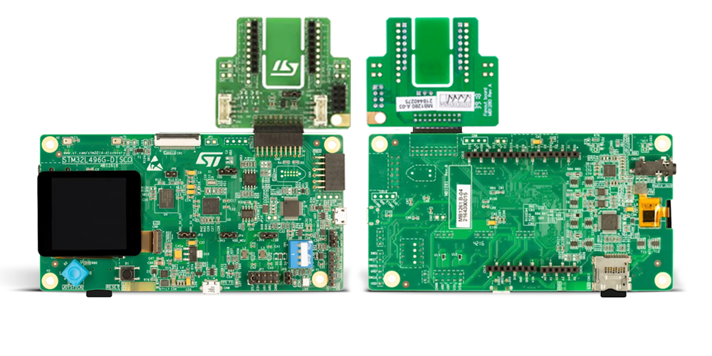
开发板
32L496GDISCOVERY Discovery 套件是一款功能全面的演示和开发平台,专为搭载 Arm® Cortex®-M4 内核的 STM32L496AG 微控制器设计。该套件适用于需要在高性能、先进图形处理和超低功耗之间取得平衡的应用,支持无缝原型开发,适用于各种嵌入式解决方案。STM32L496AG 采用创新的节能架构,集成
了扩展 RAM 和 Chrom-ART 图形加速器,在提升图形性能的同时保持低功耗,使其特别适用于音频处理、图形用户界面和实时数据采集等对能效要求较高的应用。为了简化开发流程,该开发板配备了板载 ST-LINK/V2-1 调试器/编程器,提供即插即用的调试和编程体验,使用户无需额外硬件即可轻松加载、调
试和测试应用程序。凭借低功耗特性、增强的内存能力以及内置调试工具,32L496GDISCOVERY 套件是开发先进嵌入式系统、实现高效能解决方案的理想选择。
微控制器概述
MCU卡片 / MCU
建筑
ARM Cortex-M4
MCU 内存 (KB)
1024
硅供应商
STMicroelectronics
引脚数
169
RAM (字节)
327680
使用的MCU引脚
mikroBUS™映射器
“仔细看看!”
Click board™ 原理图

一步一步来
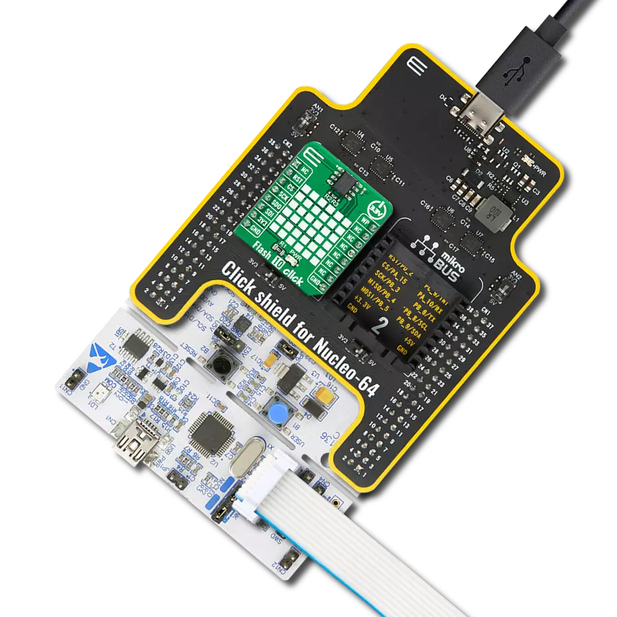
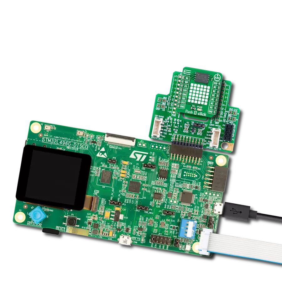
项目组装
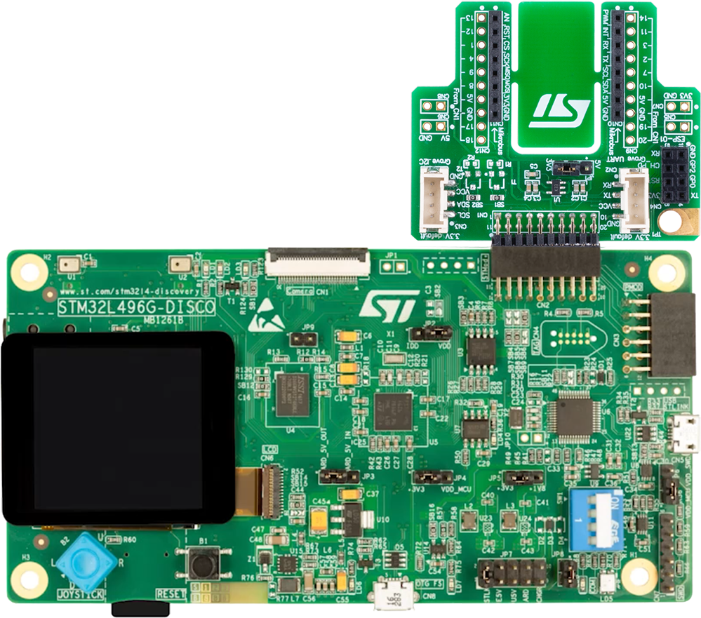
从选择您的开发板和Click板™开始。以Discovery kit with STM32L496AG MCU作为您的开发板开始。


实时跟踪您的结果
应用程序输出
1. 应用程序输出 - 在调试模式下,“应用程序输出”窗口支持实时数据监控,直接提供执行结果的可视化。请按照提供的教程正确配置环境,以确保数据正确显示。

2. UART 终端 - 使用UART Terminal通过USB to UART converter监视数据传输,实现Click board™与开发系统之间的直接通信。请根据项目需求配置波特率和其他串行设置,以确保正常运行。有关分步设置说明,请参考提供的教程。

3. Plot 输出 - Plot功能提供了一种强大的方式来可视化实时传感器数据,使趋势分析、调试和多个数据点的对比变得更加直观。要正确设置,请按照提供的教程,其中包含使用Plot功能显示Click board™读数的分步示例。在代码中使用Plot功能时,请使用以下函数:plot(insert_graph_name, variable_name);。这是一个通用格式,用户需要将“insert_graph_name”替换为实际图表名称,并将“variable_name”替换为要显示的参数。

软件支持
库描述
该库包含 Flash 8 Click 驱动程序的 API。
关键功能:
flash8_write_memory- Flash 8 写入内存函数。flash8_read_memory- Flash 8 读取内存函数。flash8_read_id- Flash 8 读取 ID 函数。
开源
代码示例
完整的应用程序代码和一个现成的项目可以通过NECTO Studio包管理器直接安装到NECTO Studio。 应用程序代码也可以在MIKROE的GitHub账户中找到。
/*!
 * @file main.c
 * @brief Flash8 Click example
 *
 * # Description
 * This library contains API for Flash 8 Click driver.
 * The library using SPI serial interface.
 * The library also includes a function for write and read memory
 * as well as write protection control functions.
 *
 * The demo application is composed of two sections :
 *
 * ## Application Init
 * Initialization of SPI module and log UART.
 * After driver initialization and default setting,
 * involves disabling write protection and hold,
 * the app writes demo_data string ( mikroE ) starting
 * from the selected row_address of the 123 ( 0x0000007B )
 * and column_address of the 456 ( 0x01C8 ).
 *
 * ## Application Task
 * This is an example that shows the use of a Flash 8 Click board™.
 * The app reads a data string, which we have previously written to memory,
 * starting from the selected row_address of the 123 ( 0x0000007B )
 * and column_address of the 456 ( 0x01C8 ).
 * Results are being sent to the Usart Terminal where you can track their changes.
 *
 * @author Nenad Filipovic
 *
 */

#include "board.h"
#include "log.h"
#include "flash8.h"

static flash8_t flash8;
static log_t logger;

static uint8_t manufacture_id;
static uint8_t device_id;
static uint8_t organization_id;
static uint8_t feature_status_out;
static uint8_t demo_data[ 9 ] = { 'M', 'i', 'k', 'r', 'o', 'E', 13 ,10 , 0 };
static uint8_t rx_data[ 9 ] = { 0 };
static feature_cfg_t feature_data;

void application_init ( void )
{
    log_cfg_t log_cfg;        /**< Logger config object. */
    flash8_cfg_t flash8_cfg;  /**< Click config object. */

    /**
     * Logger initialization.
     * Default baud rate: 115200
     * Default log level: LOG_LEVEL_DEBUG
     * @note If USB_UART_RX and USB_UART_TX
     * are defined as HAL_PIN_NC, you will
     * need to define them manually for log to work.
     * See @b LOG_MAP_USB_UART macro definition for detailed explanation.
     */
    LOG_MAP_USB_UART( log_cfg );
    log_init( &logger, &log_cfg );
    log_info( &logger, " Application Init " );

    // Click initialization.
    flash8_cfg_setup( &flash8_cfg );
    FLASH8_MAP_MIKROBUS( flash8_cfg, MIKROBUS_1 );
    if ( SPI_MASTER_ERROR == flash8_init( &flash8, &flash8_cfg ) )
    {
        log_error( &logger, " Application Init Error. " );
        log_info( &logger, " Please, run program again... " );
        for ( ; ; );
    }

    flash8_default_cfg ( &flash8 );
    log_info( &logger, " Application Task " );
    Delay_ms ( 100 );

    flash8_read_id( &flash8, &manufacture_id, &device_id, &organization_id );
    log_printf( &logger, "--------------------------\r\n" );
    log_printf( &logger, "  Manufacture ID  : 0x%.2X\r\n", ( uint16_t) manufacture_id );
    log_printf( &logger, "  Device ID       : 0x%.2X\r\n", ( uint16_t) device_id );
    log_printf( &logger, "  Organization ID : 0x%.2X\r\n", ( uint16_t) organization_id );
    log_printf( &logger, "--------------------------\r\n" );
    Delay_ms ( 100 );

    flash8_sw_reset( &flash8, &feature_status_out );
    if ( feature_status_out & FLASH8_GET_PRG_F_PROGRAM_FAIL )
    {
        log_printf( &logger, "\tProgram Fail \r\n" );
    }
    else
    {
        log_printf( &logger, "\tProgram Pass \r\n" );
    }
    log_printf( &logger, "--------------------------\r\n" );
    Delay_ms ( 1000 );

    feature_data.brwd   = FLASH8_SET_BRWD_ENABLE;
    feature_data.bl     = FLASH8_SET_BL_ALL_UNLOCKED;
    feature_data.idr_e  = FLASH8_SET_IDR_E_NORMAL_OPERATION;
    feature_data.ecc_e  = FLASH8_SET_ECC_E_INTERNAL_ECC_ENABLE;
    feature_data.prt_e  = FLASH8_SET_PRT_E_NORMAL_OPERATION;
    feature_data.hse    = FLASH8_SET_HSE_HIGH_SPEED_MODE_ENABLE;
    feature_data.hold_d = FLASH8_SET_HOLD_D_HOLD_IS_ENABLED;
    feature_data.wel    = FLASH8_SET_WEL_WRITE_ENABLE;
    flash8_set_config_feature( &flash8, feature_data );
    Delay_ms ( 100 );

    flash8_block_erase( &flash8, 123, &feature_status_out );
    if ( feature_status_out & FLASH8_GET_ERS_F_ERASE_FAIL )
    {
        log_printf( &logger, "\tErase Fail \r\n" );
    }
    else
    {
        log_printf( &logger, "\tErase Pass \r\n" );
    }
    log_printf( &logger, "--------------------------\r\n" );
    Delay_ms ( 1000 );

    log_printf( &logger, "   Write data : %s", demo_data );
    log_printf( &logger, "--------------------------\r\n" );
    log_printf( &logger, "        Write status:\r\n"  );
    flash8_write_memory( &flash8, 123, 456, &demo_data[ 0 ], 9, &feature_status_out );
    if ( feature_status_out & FLASH8_GET_OIP_BUSY_STATE )
    {
        log_printf( &logger, " Operation is in progress.\r\n" );
    }
    else
    {
        log_printf( &logger, " Operation is not in progress.\r\n" );
    }
    log_printf( &logger, "- - - - - - - - - - -  - -\r\n" );
    Delay_ms ( 1000 );

    log_printf( &logger, "    Check data ready...\r\n" );
    while ( FLASH8_GET_OIP_READY_STATE != feature_status_out )
    {
        flash8_get_feature( &flash8, FLASH8_FEATURE_C0, &feature_status_out );
        log_printf( &logger, "\tBusy state.\r\n" );
        Delay_ms ( 100 );
    }

    if ( FLASH8_GET_OIP_READY_STATE == feature_status_out )
    {
        log_printf( &logger, "\tReady state.\r\n" );
    }
    log_printf( &logger, "--------------------------\r\n" );
    Delay_ms ( 100 );
}

void application_task ( void )
{
    flash8_read_memory( &flash8, 123, 456, &rx_data[ 0 ], 9, &feature_status_out );
    log_printf( &logger, "    Read data : %s", rx_data );
    log_printf( &logger, "--------------------------\r\n" );
    Delay_ms ( 1000 );
    Delay_ms ( 1000 );
}

int main ( void )
{
    /* Do not remove this line or clock might not be set correctly. */
    #ifdef PREINIT_SUPPORTED
    preinit();
    #endif

    application_init( );

    for ( ; ; )
    {
        application_task( );
    }

    return 0;
}

// ------------------------------------------------------------------------ END
额外支持
资源
类别:闪存