使用 AD74412R 和 MK64FN1M0VDC12 提升系统性能
紧凑而强大

已发布 6月 24, 2024
点击板
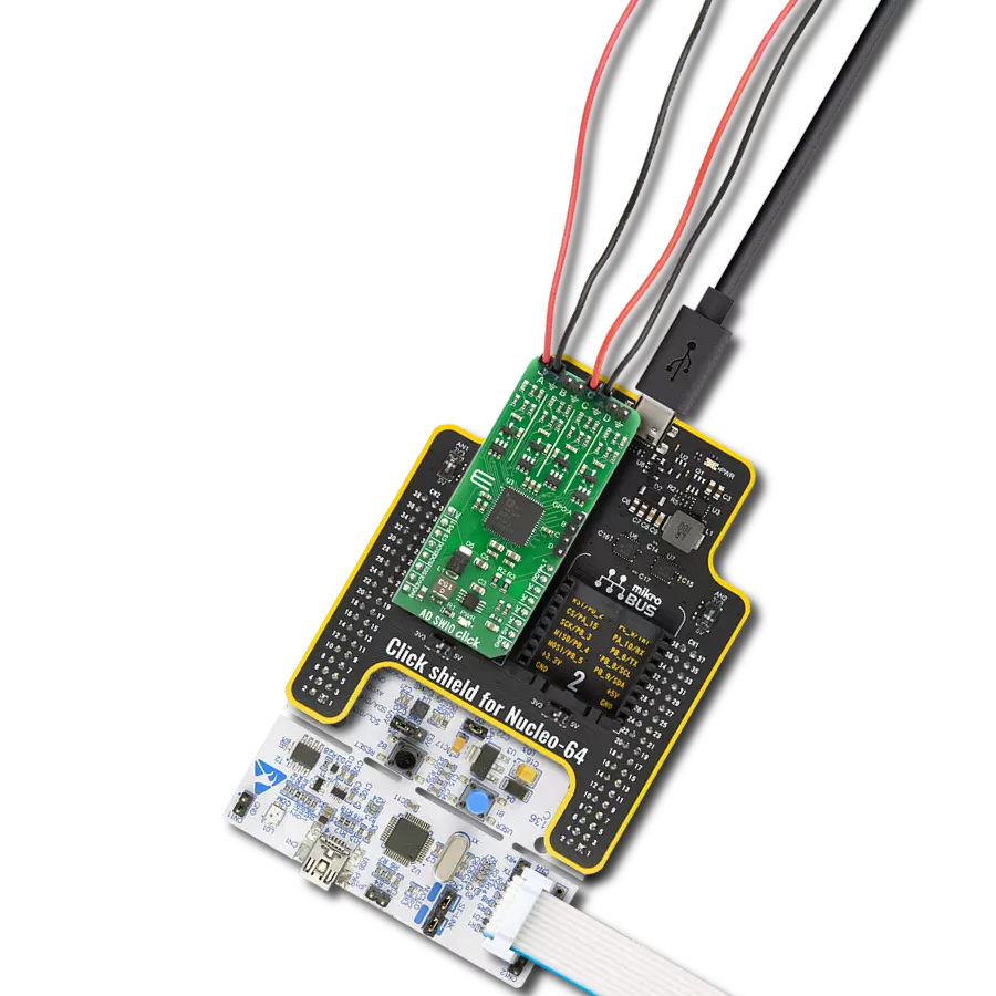
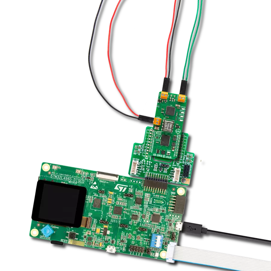
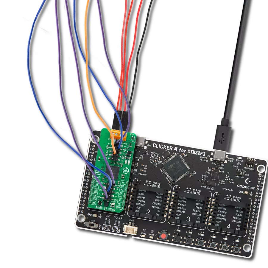
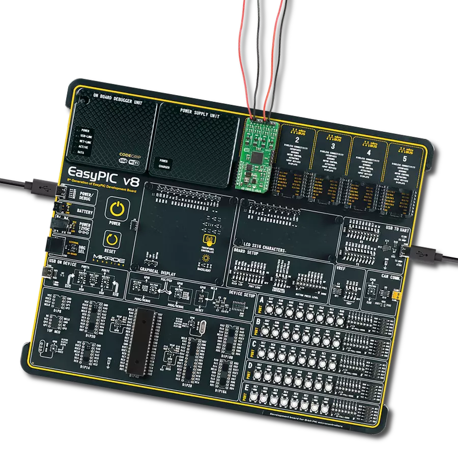
AD-SWIO Click
开发板
Clicker 2 for Kinetis
编译器
NECTO Studio
微控制器单元
MK64FN1M0VDC12
对于需要同时执行ADC和DAC功能的应用而言,这是一款颠覆性的产品。
A
A
硬件概览
它是如何工作的?
AD-SWIO Click 基于Analog Devices的AD74412R,这是一款16位模数转换器(ADC)和13位数模转换器(DAC)。AD74412R有多种模式,包括电压输出、电流输出、电压输入、外部供电电流输入、环路供电电流输入、外部RTD测量、数字输入逻辑和环路供电数字输入。ADC可以测量100Ω RSENSE上的电压或各通道I/OP_x接线端子上的电压。在高阻抗模式下,ADC默认测量接线端子(I/OP_x到I/ON_x)上的电压,范围为0V到10V。ADC还提供用户可选输入的诊断信息,如电源、内部芯片温度、参考和稳压器。AD-SWIO Click有四个GPO-x引脚,每个通道一个(GPO-A、
GPO-B、GPO-C、GPO-D)。每个通道的GPO-x引脚可以配置为数字输入功能的逻辑输出或高低电平输出。可以通过GPO_CONFIGx寄存器中的GPO_SELECT位设置GPO-x引脚。Click板™还包含一个LVIN(低电压输入)引脚,该引脚上的测量电压范围为0V到2.5V。AD74412R有四个13位DAC,每个通道一个。每个DAC核心是一个13位串DAC。架构结构包括一串电阻器,每个电阻器的值为R。加载到DAC_CODEx寄存器的数字输入码确定从哪个串节点分接电压并送入输出放大器。该架构本质上是单调且线性的。AD74412R在电压输出模式下具有可编程的短路限制,每个通道都可以编
程。该电路在AVDD电源上升或使用情况配置更改时,最小化I/OP_x接线端子的毛刺。可以通过AVDD引脚上的正向模拟电源来调节此短路限制。AD-SWIO 2 Click的输出电压限制为+20V。AD-SWIO 2 Click配备了Analog Devices的ADP1613升压DC-DC开关转换器,带有集成电源开关,能够提供高达20V的输出电压。此Click板™只能在3.3V逻辑电压水平下运行。在使用具有不同逻辑电平的MCU之前,板上必须执行适当的逻辑电压电平转换。然而,该Click板™配有一个库,包含功能和示例代码,可以用作进一步开发的参考。

功能概述
开发板
Clicker 2 for Kinetis 是一款紧凑型入门开发板,它将 Click 板™的灵活性带给您喜爱的微控制器,使其成为实现您想法的完美入门套件。它配备了一款板载 32 位 ARM Cortex-M4F 微控制器,NXP 半导体公司的 MK64FN1M0VDC12,两个 mikroBUS™ 插槽用于 Click 板™连接,一个 USB 连接器,LED 指示灯,按钮,一个 JTAG 程序员连接器以及两个 26 针头用于与外部电子设备的接口。其紧凑的设计和清晰、易识别的丝网标记让您能够迅速构建具有独特功能和特性
的小工具。Clicker 2 for Kinetis 开发套件的每个部分 都包含了使同一板块运行最高效的必要组件。除了可以选择 Clicker 2 for Kinetis 的编程方式,使用 USB HID mikroBootloader 或外部 mikroProg 连接器进行 Kinetis 编程外,Clicker 2 板还包括一个干净且调节过的开发套件电源供应模块。它提供了两种供电方式;通过 USB Micro-B 电缆,其中板载电压调节器为板上每个组件提供适当的电压水平,或使用锂聚合物 电池通过板载电池连接器供电。所有 mikroBUS™ 本
身支持的通信方法都在这块板上,包括已经建立良好的 mikroBUS™ 插槽、重置按钮和几个用户可配置的按钮及 LED 指示灯。Clicker 2 for Kinetis 是 Mikroe 生态系统的一个组成部分,允许您在几分钟内创建新的应用程序。它由 Mikroe 软件工具原生支持,得益于大量不同的 Click 板™(超过一千块板),其数量每天都在增长,它涵盖了原型制作的许多方面。

微控制器概述
MCU卡片 / MCU

建筑
ARM Cortex-M4
MCU 内存 (KB)
1024
硅供应商
NXP
引脚数
121
RAM (字节)
262144
使用的MCU引脚
mikroBUS™映射器
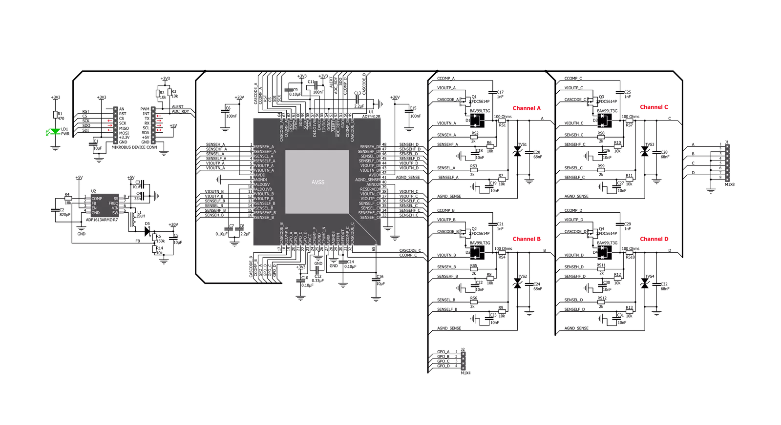
“仔细看看!”
Click board™ 原理图
一步一步来
项目组装

从选择您的开发板和Click板™开始。以Clicker 2 for Kinetis作为您的开发板开始。


软件支持
库描述
该库包含 AD-SWIO Click 驱动程序的 API。
关键功能:
adswio_status_pin_ready- 此函数检查就绪引脚的状态。adswio_get_conv_results- 此函数允许用户获取所选通道的转换结果。
开源
代码示例
完整的应用程序代码和一个现成的项目可以通过NECTO Studio包管理器直接安装到NECTO Studio。 应用程序代码也可以在MIKROE的GitHub账户中找到。
/*!
 * \file
 * \brief AdSwio Click example
 *
 * # Description
 * This Click provides a fully integrated single chip solution for input and output operation.
 * The AD-SWIO Click contains four 13-bit DACs, one per chanal, and 16-bit Σ-∆ ADC.
 * These options give a lot of flexibility in choosing functionality for analog output,
 * analog input, digital input, resistance temperature detector (RTD), and thermocouple
 * measurements integrated into a single chip solution with a serial peripheral interface (SPI).
 *
 * The demo application is composed of two sections :
 *
 * ## Application Init
 * Performs a hardware reset of the Click board and
 * executes a default configuration that enables channel A and sets it to measure voltage
 * input in the range from 0V to 10V, with 4800 SPS.
 *
 * ## Application Task
 * Waits for the data ready and then reads the results of ADC conversion from channel A
 * and if response is ok, then prints the results on the uart console.
 *
 * ## Additional Functions
 *
 * - void application_default_handler ( uint8_t *err_msg ) - Sends an error report messages from Click
 * driver to initialized console module. It must be set using adswio2_set_handler function.
 *
 *
 * \author MikroE Team
 *
 */
// ------------------------------------------------------------------- INCLUDES

#include "board.h"
#include "log.h"
#include "adswio.h"

// ------------------------------------------------------------------ VARIABLES

static adswio_t adswio;
static log_t logger;

static uint8_t adswio_rdy;
static adswio_err_t adswio_err;
static uint16_t adswio_ch_a;
static float adswio_res;

const uint16_t ADSWIO_RANGE_VOLT_MV = 10000;
const uint32_t ADSWIO_RANGE_RESOLUTION = 65536;

// ------------------------------------------------------ ADDITIONAL FUNCTIONS

void application_default_handler ( uint8_t *err_msg )
{
    char *err_ptr = err_msg;

    log_printf( &logger, "\r\n" );
    log_printf( &logger, "[ERROR] : %s", err_ptr );
    log_printf( &logger, "\r\n" );
}

// ------------------------------------------------------ APPLICATION FUNCTIONS

void application_init ( void )
{
    log_cfg_t log_cfg;
    adswio_cfg_t cfg;

    /**
     * Logger initialization.
     * Default baud rate: 115200
     * Default log level: LOG_LEVEL_DEBUG
     * @note If USB_UART_RX and USB_UART_TX
     * are defined as HAL_PIN_NC, you will
     * need to define them manually for log to work.
     * See @b LOG_MAP_USB_UART macro definition for detailed explanation.
     */
    LOG_MAP_USB_UART( log_cfg );
    log_init( &logger, &log_cfg );
    log_info( &logger, "---- Application Init ----" );

    //  Click initialization.

    adswio_cfg_setup( &cfg );
    ADSWIO_MAP_MIKROBUS( cfg, MIKROBUS_1 );
    adswio_init( &adswio, &cfg );
    Delay_ms ( 100 );

    adswio_default_cfg( &adswio );
    Delay_ms ( 1000 );

    adswio_rdy  = DUMMY;
    adswio_ch_a = DUMMY;
    adswio_res  = DUMMY;
    adswio_err  = ADSWIO_ERR_STATUS_OK;

    log_printf( &logger, " AD-SWIO Click initialization done \r\n");
    log_printf( &logger, "************************************\r\n");
}

void application_task ( void )
{
    uint16_t timeout = 0;
    do
    {
        Delay_1ms( );
        timeout++;
        adswio_rdy = adswio_status_pin_ready( &adswio );
        if ( timeout > 3000 )
        {
            timeout = 0;
            log_printf( &logger, " Reinitializing...");
            adswio_default_cfg( &adswio );
            log_printf( &logger, "Done\r\n");
        }
    }
    while ( adswio_rdy != 0 );

    adswio_err = adswio_get_conv_results( &adswio, ADSWIO_SETUP_CONV_EN_CHA, &adswio_ch_a );

    if ( adswio_err == ADSWIO_ERR_STATUS_OK )
    {
        adswio_res = adswio_ch_a;
        adswio_res /= ADSWIO_RANGE_RESOLUTION;
        adswio_res *= ADSWIO_RANGE_VOLT_MV;
        adswio_ch_a = adswio_res;

        log_printf( &logger, " Voltage from channel A: %d mV\r\n", adswio_ch_a );

        log_printf( &logger, "-----------------------------------\r\n\r\n" );
        Delay_ms ( 200 );
    }
}

int main ( void )
{
    /* Do not remove this line or clock might not be set correctly. */
    #ifdef PREINIT_SUPPORTED
    preinit();
    #endif

    application_init( );

    for ( ; ; )
    {
        application_task( );
    }

    return 0;
}


// ------------------------------------------------------------------------ END