Experience LTE Cat 1bis communication for American region with the LEXI-R10401D and STM32G474RE
LTE Cat 1bis connectivity with integrated geolocation for American IoT solutions
Published Jun 18, 2025
Click board™
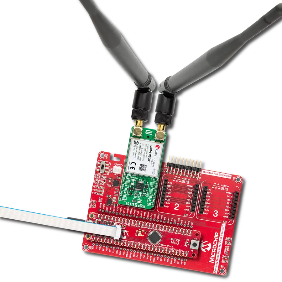
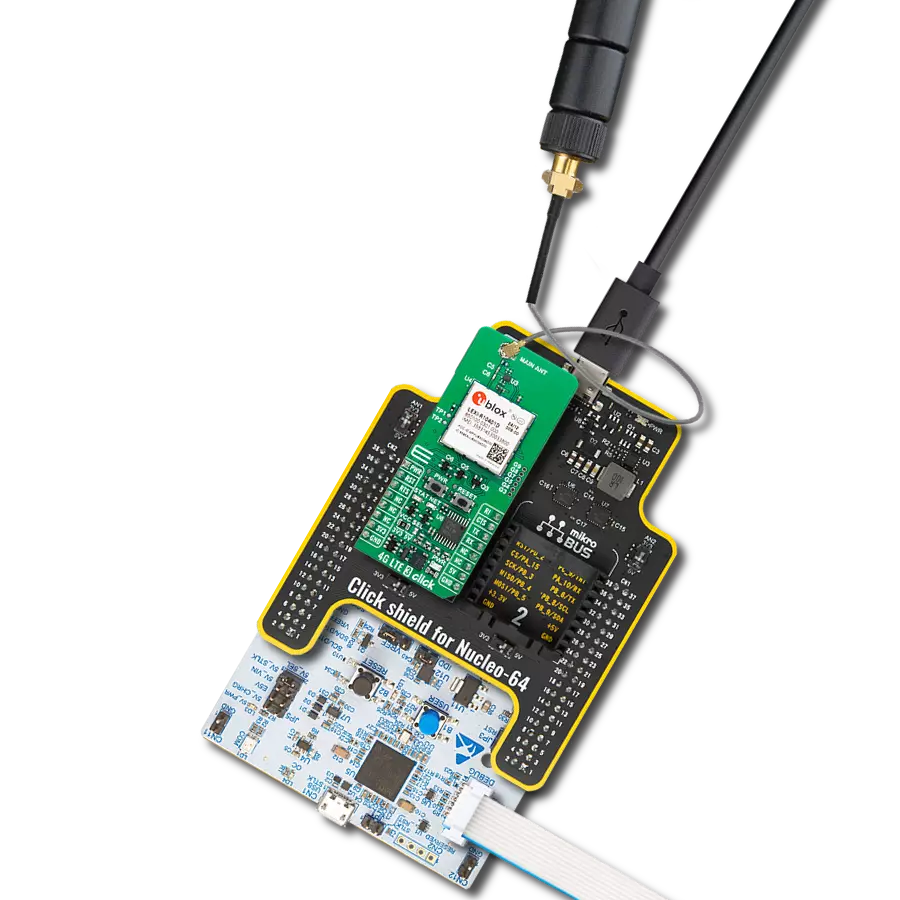
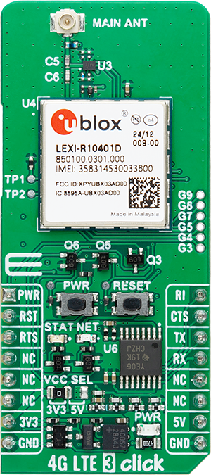
4G LTE 3 Click (for North America)
Dev. board
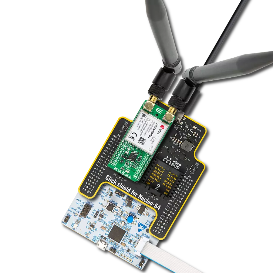
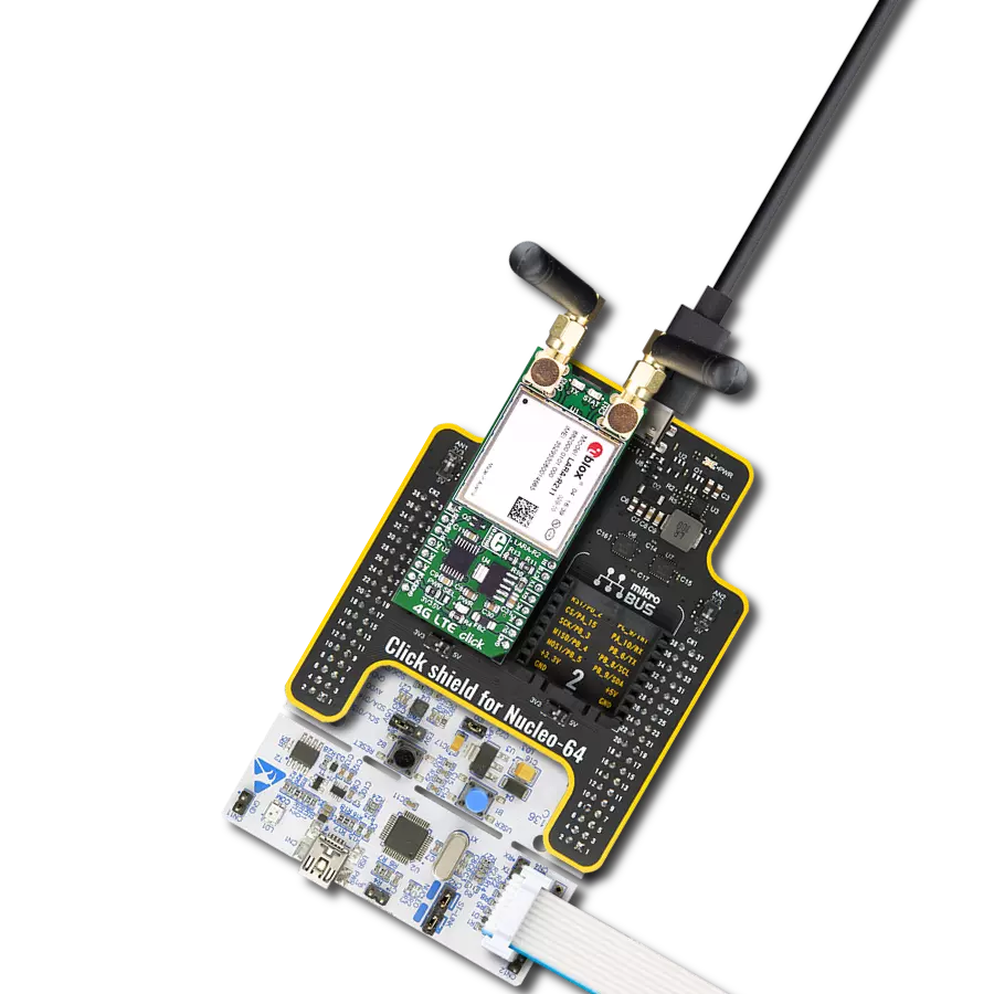
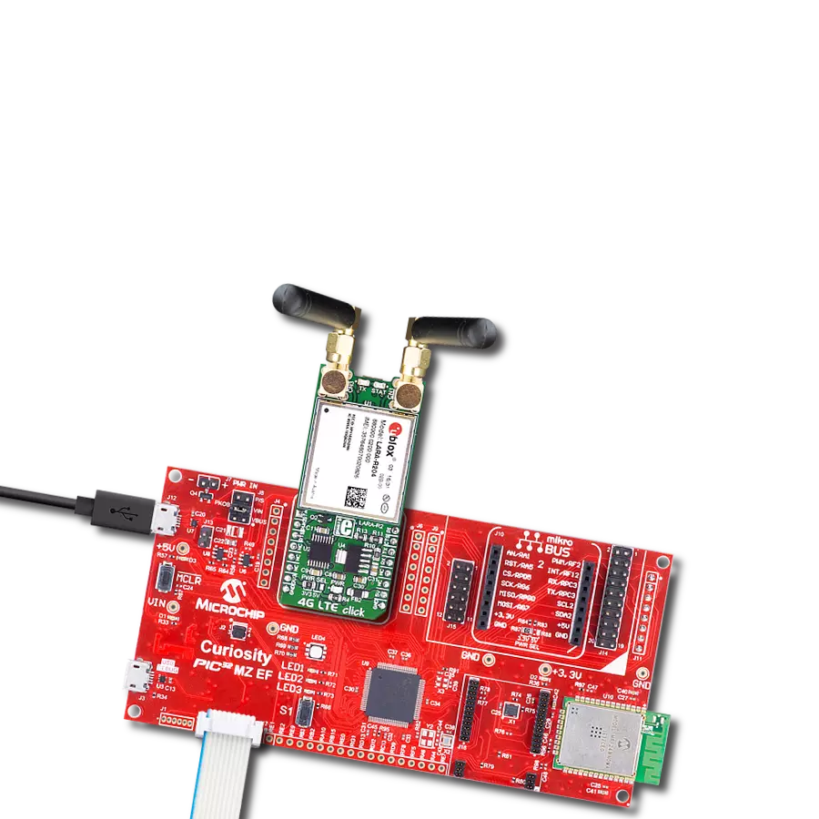
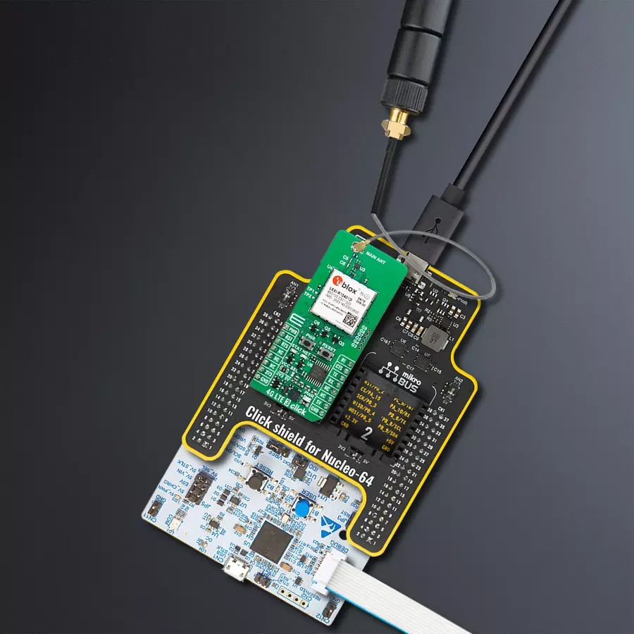
Nucleo 64 with STM32G474RE MCU
Compiler
NECTO Studio
MCU
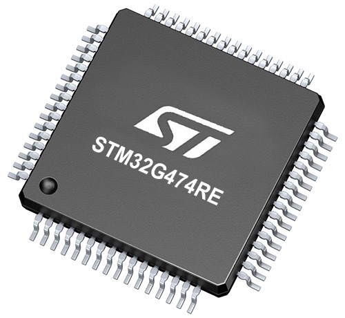
STM32G474RE
LTE Cat 1bis connectivity with indoor positioning support ideal for asset tracking, telematics, and wearables across North America
A
A
Hardware Overview
How does it work?
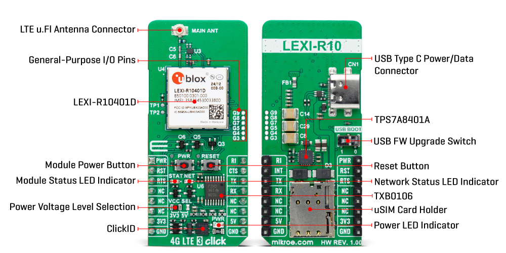
4G LTE 3 Click (for North America) is based on the LEXI-R10401D, a single-mode LTE Cat 1bis module from Trasna, made for applications requiring reliable connectivity, medium data speeds, and extensive coverage in the American regions. The LEXI-R10401D module is designed to meet professional-grade standards, adhering to the Trasna qualification policy and the stringent AEC-Q104 standard. It supports various LTE FDD bands, including 2, 4, 5, 12, 13, 14, 66, and 71 ensuring broad compatibility and superior performance across multiple regional networks. Additionally, the module has regulatory certifications such as PTCRB, GCF, FCC, ISED, AT&T, Verizon, and FirstNet, allowing deployment across supported markets. Beyond its LTE functionality, the LEXI-R10401D integrates an embedded Wi-Fi scan, enabling the scanning of Wi-Fi hotspots for enhanced indoor positioning, and supports the Trasna CellLocate® service for advanced geolocation capabilities. This compact and highly integrated module offers medium-capacity data connectivity, achieving download speeds of up to 10Mbps and upload speeds of 5Mbps, all while maintaining exceptionally low power consumption. These features make it an ideal choice for cost-sensitive applications that demand moderate data speeds and reliable coverage. Its versatile use cases include asset tracking, telematics, healthcare devices, and wearables, where efficient and robust connectivity
is paramount. Communication between the LEXI-R10401D and the host MCU is made through a UART interface, using standard UART RX and TX pins and hardware flow control pins (CTS/RTS/RI - Clear to Send/Ready to Send/Ring Indicator) for efficient data transfer. The module defaults to a communication speed of 115200bps, allowing for seamless data exchange over AT commands. This Click board™ also includes a USB Type C connector for power and data transfer, which is compliant with the USB 2.0 specification with a maximum 480Mbit/s data rate (peripheral only). In addition to this interface, the board also features a USB FW upgrade switch on the back of the board labeled USB BOOT to manage firmware upgrades. This switch has positions 0 for normal operation and 1 for firmware upgrades over USB, ensuring a straightforward upgrade process. The 4G LTE 3 Click includes several additional functionalities that enhance its usability and control. The PWR button allows users to easily power the module ON or OFF, while the RESET button provides a quick way to reset the module. These functions can also be controlled digitally via the mikroBUS™ pins PWR and RST, offering greater flexibility. The board also includes an unsoldered header with six GPIO pins, allowing for further customization. Moreover, this board also has dedicated test points for diagnostic purposes, TP1 and TP2, if the host MCU uses the USB and main UART interfaces and two visual indicators to provide real-time status updates. The
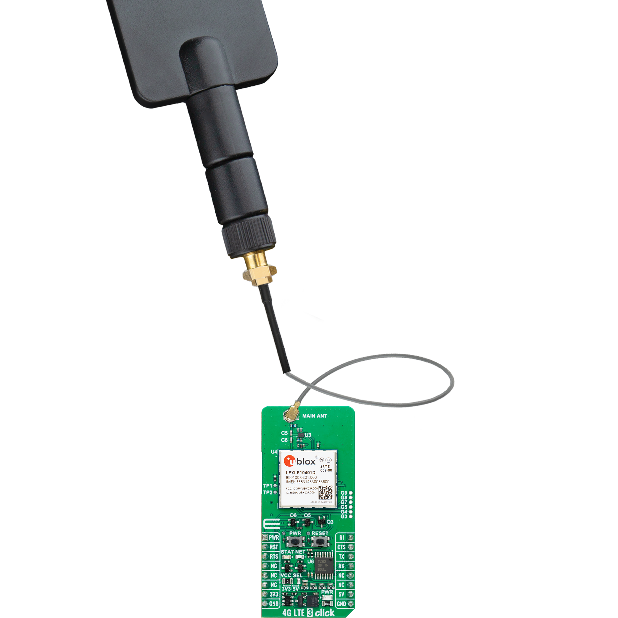
first red NET LED indicates the current network status of the module. The device has successfully registered on the network when the LED blinks slowly. If the LED blinks at a normal pace, the device has not yet registered to a network. A fast blinking pattern signals data transmission. When the LED is completely OFF, it indicates that the device is either powered OFF or in Power Saving Mode (PSM). The second yellow STAT LED indicates the module's power status, which stays off when the module is OFF and turns ON when the module is powered on or firmware ready. The board features one u.Fl connector for the main LTE antenna that MIKROE offers, like the LTE Flat Rotation Antenna combined with an IPEX-SMA cable for flexible and efficient connectivity. The board also has a micro SIM card holder that supports both 1.8V and 3.0V uSIM cards, allowing users to select the most appropriate service provider for their particular use case. This Click board™ can operate with both 3.3V and 5V logic voltage levels selected via the VCC SEL jumper. Since the LEXI-R10401D module operates at 3.8V, a logic-level translator, the TXB0106 is also used for proper operation and an accurate signal-level translation. This way, both 3.3V and 5V capable MCUs can use the communication lines properly. Also, this Click board™ comes equipped with a library containing easy-to-use functions and an example code that can be used as a reference for further development.
Features overview
Development board
Nucleo-64 with STM32G474R MCU offers a cost-effective and adaptable platform for developers to explore new ideas and prototype their designs. This board harnesses the versatility of the STM32 microcontroller, enabling users to select the optimal balance of performance and power consumption for their projects. It accommodates the STM32 microcontroller in the LQFP64 package and includes essential components such as a user LED, which doubles as an ARDUINO® signal, alongside user and reset push-buttons, and a 32.768kHz crystal oscillator for precise timing operations. Designed with expansion and flexibility in mind, the Nucleo-64 board features an ARDUINO® Uno V3 expansion connector and ST morpho extension pin
headers, granting complete access to the STM32's I/Os for comprehensive project integration. Power supply options are adaptable, supporting ST-LINK USB VBUS or external power sources, ensuring adaptability in various development environments. The board also has an on-board ST-LINK debugger/programmer with USB re-enumeration capability, simplifying the programming and debugging process. Moreover, the board is designed to simplify advanced development with its external SMPS for efficient Vcore logic supply, support for USB Device full speed or USB SNK/UFP full speed, and built-in cryptographic features, enhancing both the power efficiency and security of projects. Additional connectivity is
provided through dedicated connectors for external SMPS experimentation, a USB connector for the ST-LINK, and a MIPI® debug connector, expanding the possibilities for hardware interfacing and experimentation. Developers will find extensive support through comprehensive free software libraries and examples, courtesy of the STM32Cube MCU Package. This, combined with compatibility with a wide array of Integrated Development Environments (IDEs), including IAR Embedded Workbench®, MDK-ARM, and STM32CubeIDE, ensures a smooth and efficient development experience, allowing users to fully leverage the capabilities of the Nucleo-64 board in their projects.

Microcontroller Overview
MCU Card / MCU
Architecture
ARM Cortex-M4
MCU Memory (KB)
512
Silicon Vendor
STMicroelectronics
Pin count
64
RAM (Bytes)
128k
You complete me!
Accessories
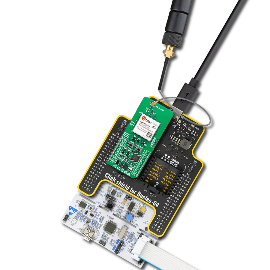
Click Shield for Nucleo-64 comes equipped with two proprietary mikroBUS™ sockets, allowing all the Click board™ devices to be interfaced with the STM32 Nucleo-64 board with no effort. This way, Mikroe allows its users to add any functionality from our ever-growing range of Click boards™, such as WiFi, GSM, GPS, Bluetooth, ZigBee, environmental sensors, LEDs, speech recognition, motor control, movement sensors, and many more. More than 1537 Click boards™, which can be stacked and integrated, are at your disposal. The STM32 Nucleo-64 boards are based on the microcontrollers in 64-pin packages, a 32-bit MCU with an ARM Cortex M4 processor operating at 84MHz, 512Kb Flash, and 96KB SRAM, divided into two regions where the top section represents the ST-Link/V2 debugger and programmer while the bottom section of the board is an actual development board. These boards are controlled and powered conveniently through a USB connection to program and efficiently debug the Nucleo-64 board out of the box, with an additional USB cable connected to the USB mini port on the board. Most of the STM32 microcontroller pins are brought to the IO pins on the left and right edge of the board, which are then connected to two existing mikroBUS™ sockets. This Click Shield also has several switches that perform functions such as selecting the logic levels of analog signals on mikroBUS™ sockets and selecting logic voltage levels of the mikroBUS™ sockets themselves. Besides, the user is offered the possibility of using any Click board™ with the help of existing bidirectional level-shifting voltage translators, regardless of whether the Click board™ operates at a 3.3V or 5V logic voltage level. Once you connect the STM32 Nucleo-64 board with our Click Shield for Nucleo-64, you can access hundreds of Click boards™, working with 3.3V or 5V logic voltage levels.

LTE Flat Rotation Antenna is a versatile choice for boosting the performance of 3G/4G LTE devices. With a wide frequency range of 700-2700MHz, it ensures optimal connectivity on major cellular bands worldwide. This flat antenna features an SMA male connector, making it easy to attach directly to your device or SMA module connector. One of its standout features is its adjustable angle, which can be set in 45⁰ increments (0⁰/45⁰/90⁰), allowing you to fine-tune the antenna's orientation for maximum signal reception. With an impedance of 50Ω and a VSW Ratio of <2.0:1, this antenna ensures a reliable and efficient connection. Its 5dB gain, vertical polarization, and omnidirectional radiation pattern enhance signal strength, making it suitable for various applications. Measuring 196mm in length and 38mm in width, this antenna offers a compact yet effective solution for improving your connectivity. With a maximum input power of 50W, it can handle the demands of various devices.

IPEX-SMA cable is a type of RF (radio frequency) cable assembly. "IPEX" refers to the IPEX connector, a miniature coaxial connector commonly used in small electronic devices. "SMA" stands for SubMiniature Version A and is another coaxial connector commonly used in RF applications. An IPEX-SMA cable assembly has an IPEX connector on one end and an SMA connector on the other, allowing it to connect devices or components that use these specific connectors. These cables are often used in applications like WiFi or cellular antennas, GPS modules, and other RF communication systems where a reliable and low-loss connection is required.

Used MCU Pins
mikroBUS™ mapper
Take a closer look
Click board™ Schematic

Step by step
Project assembly
Start by selecting your development board and Click board™. Begin with the Nucleo 64 with STM32G474RE MCU as your development board.


Software Support
Library Description
4G LTE 3 Click (for North America) demo application is developed using the NECTO Studio, ensuring compatibility with mikroSDK's open-source libraries and tools. Designed for plug-and-play implementation and testing, the demo is fully compatible with all development, starter, and mikromedia boards featuring a mikroBUS™ socket.
Example Description
Application example shows device capability of connecting to the network and sending SMS or TCP/UDP messages using standard "AT" commands.
Key functions:
c4glte3na_cfg_setup- Config Object Initialization function.c4glte3na_init- Initialization function.c4glte3na_set_sim_apn- This function sets APN for sim card.c4glte3na_send_sms_text- This function sends text message to a phone number.c4glte3na_cmd_run- This function sends a specified command to the Click module.
Application Init
Initializes the driver and logger.
Application Task
Application task is split in few stages:
C4GLTE3NA_POWER_UP:Powers up the device, performs a factory reset and reads system information.C4GLTE3NA_CONFIG_CONNECTION:Sets configuration to device to be able to connect to the network.C4GLTE3NA_CHECK_CONNECTION:Waits for the network registration indicated via CEREG command and then checks the signal quality report.C4GLTE3NA_CONFIG_EXAMPLE:Configures device for the selected example.C4GLTE3NA_EXAMPLE:Depending on the selected demo example, it sends an SMS message (in PDU or TXT mode) or TCP/UDP message. By default, the TCP/UDP example is selected.
Open Source
Code example
The complete application code and a ready-to-use project are available through the NECTO Studio Package Manager for direct installation in the NECTO Studio. The application code can also be found on the MIKROE GitHub account.
/*!
 * @file main.c
 * @brief 4G LTE 3 NA Click Example.
 *
 * # Description
 * Application example shows device capability of connecting to the network and
 * sending SMS or TCP/UDP messages using standard "AT" commands.
 *
 * The demo application is composed of two sections :
 *
 * ## Application Init
 * Initializes the driver and logger.
 *
 * ## Application Task
 * Application task is split in few stages:
 *  - C4GLTE3NA_POWER_UP:
 * Powers up the device, performs a factory reset and reads system information.
 *
 *  - C4GLTE3NA_CONFIG_CONNECTION:
 * Sets configuration to device to be able to connect to the network.
 *
 *  - C4GLTE3NA_CHECK_CONNECTION:
 * Waits for the network registration indicated via CEREG command and then checks
 * the signal quality report.
 *
 *  - C4GLTE3NA_CONFIG_EXAMPLE:
 * Configures device for the selected example.
 *
 *  - C4GLTE3NA_EXAMPLE:
 * Depending on the selected demo example, it sends an SMS message (in PDU or TXT mode) or TCP/UDP message.
 *
 * By default, the TCP/UDP example is selected.
 *
 * ## Additional Function
 * - static void c4glte3na_clear_app_buf ( void )
 * - static void c4glte3na_log_app_buf ( void )
 * - static err_t c4glte3na_process ( c4glte3na_t *ctx )
 * - static err_t c4glte3na_read_response ( c4glte3na_t *ctx, uint8_t *rsp )
 * - static err_t c4glte3na_power_up ( c4glte3na_t *ctx )
 * - static err_t c4glte3na_config_connection ( c4glte3na_t *ctx )
 * - static err_t c4glte3na_check_connection ( c4glte3na_t *ctx )
 * - static err_t c4glte3na_config_example ( c4glte3na_t *ctx )
 * - static err_t c4glte3na_example ( c4glte3na_t *ctx )
 *
 * @note
 * In order for the examples to work, user needs to set the APN and SMSC (SMS PDU mode only)
 * of entered SIM card as well as the phone number (SMS mode only) to which he wants to send an SMS.
 * Enter valid values for the following macros: SIM_APN, SIM_SMSC and PHONE_NUMBER.
 * Example:
    SIM_APN "internet"
    SIM_SMSC "+381610401"
    PHONE_NUMBER "+381659999999"
 *
 * @author Stefan Filipovic
 *
 */

#include "board.h"
#include "log.h"
#include "c4glte3na.h"
#include "generic_pointer.h"
#include "conversions.h"

// Example selection macros
#define EXAMPLE_TCP_UDP                     0               // Example of sending messages to a TCP/UDP echo server
#define EXAMPLE_SMS                         1               // Example of sending SMS to a phone number
#define DEMO_EXAMPLE                        EXAMPLE_TCP_UDP // Example selection macro

// SIM APN config
#define SIM_APN                             "internet"      // Set valid SIM APN

// SMS example parameters
#define SIM_SMSC                            ""              // Set valid SMS Service Center Address - only in SMS PDU mode
#define PHONE_NUMBER                        ""              // Set Phone number to message
#define SMS_MODE                            "1"             // SMS mode: "0" - PDU, "1" - TXT

// TCP/UDP example parameters
#define REMOTE_IP                           "77.46.162.162" // TCP/UDP echo server IP address
#define REMOTE_PORT                         "51111"         // TCP/UDP echo server port

// Message content
#define MESSAGE_CONTENT                     "4G LTE 3 NA Click board - demo example."

// Application buffer size
#define APP_BUFFER_SIZE                     256
#define PROCESS_BUFFER_SIZE                 256

/**
 * @brief Example states.
 * @details Predefined enum values for application example state.
 */
typedef enum
{
    C4GLTE3NA_POWER_UP = 1,
    C4GLTE3NA_CONFIG_CONNECTION,
    C4GLTE3NA_CHECK_CONNECTION,
    C4GLTE3NA_CONFIG_EXAMPLE,
    C4GLTE3NA_EXAMPLE

} c4glte3na_app_state_t;

/**
 * @brief Application example variables.
 * @details Variables used in application example.
 */
static uint8_t app_buf[ APP_BUFFER_SIZE ] = { 0 };
static int32_t app_buf_len = 0;
static c4glte3na_app_state_t app_state = C4GLTE3NA_POWER_UP;

static c4glte3na_t c4glte3na;
static log_t logger;

/**
 * @brief 4G LTE 3 NA clearing application buffer.
 * @details This function clears memory of application buffer and reset its length.
 * @note None.
 */
static void c4glte3na_clear_app_buf ( void );

/**
 * @brief 4G LTE 3 NA log application buffer.
 * @details This function logs data from application buffer to USB UART.
 * @note None.
 */
static void c4glte3na_log_app_buf ( void );

/**
 * @brief 4G LTE 3 NA data reading function.
 * @details This function reads data from device and concatenates data to application buffer.
 * @param[in] ctx : Click context object.
 * See #c4glte3na_t object definition for detailed explanation.
 * @return @li @c  0 - Read some data.
 *         @li @c -1 - Nothing is read.
 * See #err_t definition for detailed explanation.
 * @note None.
 */
static err_t c4glte3na_process ( c4glte3na_t *ctx );

/**
 * @brief 4G LTE 3 NA read response function.
 * @details This function waits for a response message, reads and displays it on the USB UART.
 * @param[in] ctx : Click context object.
 * See #c4glte3na_t object definition for detailed explanation.
 * @param[in] rsp  Expected response.
 * @return @li @c  0 - OK response.
 *         @li @c -2 - Timeout error.
 *         @li @c -3 - Command error.
 *         @li @c -4 - Unknown error.
 * See #err_t definition for detailed explanation.
 * @note None.
 */
static err_t c4glte3na_read_response ( c4glte3na_t *ctx, uint8_t *rsp );

/**
 * @brief 4G LTE 3 NA power up function.
 * @details This function powers up the device, performs a factory reset and reads system information.
 * @param[in] ctx : Click context object.
 * See #c4glte3na_t object definition for detailed explanation.
 * @return @li @c    0 - OK.
 *         @li @c != 0 - Read response error.
 * See #err_t definition for detailed explanation.
 * @note None.
 */
static err_t c4glte3na_power_up ( c4glte3na_t *ctx );

/**
 * @brief 4G LTE 3 NA config connection function.
 * @details This function configures and enables connection to the specified network.
 * @param[in] ctx : Click context object.
 * See #c4glte3na_t object definition for detailed explanation.
 * @return @li @c    0 - OK.
 *         @li @c != 0 - Read response error.
 * See #err_t definition for detailed explanation.
 * @note None.
 */
static err_t c4glte3na_config_connection ( c4glte3na_t *ctx );

/**
 * @brief 4G LTE 3 NA check connection function.
 * @details This function checks the connection to network.
 * @param[in] ctx : Click context object.
 * See #c4glte3na_t object definition for detailed explanation.
 * @return @li @c    0 - OK.
 *         @li @c != 0 - Read response error.
 * See #err_t definition for detailed explanation.
 * @note None.
 */
static err_t c4glte3na_check_connection ( c4glte3na_t *ctx );

/**
 * @brief 4G LTE 3 NA config example function.
 * @details This function configures device for the selected example.
 * @param[in] ctx : Click context object.
 * See #c4glte3na_t object definition for detailed explanation.
 * @return @li @c    0 - OK.
 *         @li @c != 0 - Read response error.
 * See #err_t definition for detailed explanation.
 * @note None.
 */
static err_t c4glte3na_config_example ( c4glte3na_t *ctx );

/**
 * @brief 4G LTE 3 NA example function.
 * @details This function executes SMS or TCP/UDP depending on the DEMO_EXAMPLE macro.
 * @param[in] ctx : Click context object.
 * See #c4glte3na_t object definition for detailed explanation.
 * @return @li @c    0 - OK.
 *         @li @c != 0 - Read response error.
 * See #err_t definition for detailed explanation.
 * @note None.
 */
static err_t c4glte3na_example ( c4glte3na_t *ctx );

void application_init ( void )
{
    log_cfg_t log_cfg;  /**< Logger config object. */
    c4glte3na_cfg_t c4glte3na_cfg;  /**< Click config object. */

    /**
     * Logger initialization.
     * Default baud rate: 115200
     * Default log level: LOG_LEVEL_DEBUG
     * @note If USB_UART_RX and USB_UART_TX
     * are defined as HAL_PIN_NC, you will
     * need to define them manually for log to work.
     * See @b LOG_MAP_USB_UART macro definition for detailed explanation.
     */
    LOG_MAP_USB_UART( log_cfg );
    log_init( &logger, &log_cfg );
    log_info( &logger, " Application Init " );

    // Click initialization.
    c4glte3na_cfg_setup( &c4glte3na_cfg );
    C4GLTE3NA_MAP_MIKROBUS( c4glte3na_cfg, MIKROBUS_1 );
    if ( UART_ERROR == c4glte3na_init( &c4glte3na, &c4glte3na_cfg ) )
    {
        log_error( &logger, " Communication init." );
        for ( ; ; );
    }

    log_info( &logger, " Application Task " );

    app_state = C4GLTE3NA_POWER_UP;
    log_printf( &logger, ">>> APP STATE - POWER UP <<<\r\n\n" );
}

void application_task ( void )
{
    switch ( app_state )
    {
        case C4GLTE3NA_POWER_UP:
        {
            if ( C4GLTE3NA_OK == c4glte3na_power_up( &c4glte3na ) )
            {
                app_state = C4GLTE3NA_CONFIG_CONNECTION;
                log_printf( &logger, ">>> APP STATE - CONFIG CONNECTION <<<\r\n\n" );
            }
            break;
        }
        case C4GLTE3NA_CONFIG_CONNECTION:
        {
            if ( C4GLTE3NA_OK == c4glte3na_config_connection( &c4glte3na ) )
            {
                app_state = C4GLTE3NA_CHECK_CONNECTION;
                log_printf( &logger, ">>> APP STATE - CHECK CONNECTION <<<\r\n\n" );
            }
            break;
        }
        case C4GLTE3NA_CHECK_CONNECTION:
        {
            if ( C4GLTE3NA_OK == c4glte3na_check_connection( &c4glte3na ) )
            {
                app_state = C4GLTE3NA_CONFIG_EXAMPLE;
                log_printf( &logger, ">>> APP STATE - CONFIG EXAMPLE <<<\r\n\n" );
            }
            break;
        }
        case C4GLTE3NA_CONFIG_EXAMPLE:
        {
            if ( C4GLTE3NA_OK == c4glte3na_config_example( &c4glte3na ) )
            {
                app_state = C4GLTE3NA_EXAMPLE;
                log_printf( &logger, ">>> APP STATE - EXAMPLE <<<\r\n\n" );
            }
            break;
        }
        case C4GLTE3NA_EXAMPLE:
        {
            c4glte3na_example( &c4glte3na );
            break;
        }
        default:
        {
            log_error( &logger, " APP STATE." );
            break;
        }
    }
}

int main ( void )
{
    /* Do not remove this line or clock might not be set correctly. */
    #ifdef PREINIT_SUPPORTED
    preinit();
    #endif

    application_init( );

    for ( ; ; )
    {
        application_task( );
    }

    return 0;
}

static void c4glte3na_clear_app_buf ( void )
{
    memset( app_buf, 0, app_buf_len );
    app_buf_len = 0;
}

static void c4glte3na_log_app_buf ( void )
{
    for ( int32_t buf_cnt = 0; buf_cnt < app_buf_len; buf_cnt++ )
    {
        log_printf( &logger, "%c", app_buf[ buf_cnt ] );
    }
}

static err_t c4glte3na_process ( c4glte3na_t *ctx )
{
    uint8_t rx_buf[ PROCESS_BUFFER_SIZE ] = { 0 };
    int32_t overflow_bytes = 0;
    int32_t rx_cnt = 0;
    int32_t rx_size = c4glte3na_generic_read( ctx, rx_buf, PROCESS_BUFFER_SIZE );
    if ( ( rx_size > 0 ) && ( rx_size <= APP_BUFFER_SIZE ) )
    {
        if ( ( app_buf_len + rx_size ) > APP_BUFFER_SIZE )
        {
            overflow_bytes = ( app_buf_len + rx_size ) - APP_BUFFER_SIZE;
            app_buf_len = APP_BUFFER_SIZE - rx_size;
            memmove ( app_buf, &app_buf[ overflow_bytes ], app_buf_len );
            memset ( &app_buf[ app_buf_len ], 0, overflow_bytes );
        }
        for ( rx_cnt = 0; rx_cnt < rx_size; rx_cnt++ )
        {
            if ( rx_buf[ rx_cnt ] )
            {
                app_buf[ app_buf_len++ ] = rx_buf[ rx_cnt ];
            }
        }
        return C4GLTE3NA_OK;
    }
    return C4GLTE3NA_ERROR;
}

static err_t c4glte3na_read_response ( c4glte3na_t *ctx, uint8_t *rsp )
{
    #define READ_RESPONSE_TIMEOUT_MS    120000
    uint32_t timeout_cnt = 0;
    c4glte3na_clear_app_buf ( );
    c4glte3na_process( ctx );
    while ( ( 0 == strstr( app_buf, rsp ) ) &&
            ( 0 == strstr( app_buf, C4GLTE3NA_RSP_ERROR ) ) )
    {
        c4glte3na_process( ctx );
        if ( timeout_cnt++ > READ_RESPONSE_TIMEOUT_MS )
        {
            c4glte3na_clear_app_buf( );
            log_error( &logger, " Timeout!" );
            return C4GLTE3NA_ERROR_TIMEOUT;
        }
        Delay_ms( 1 );
    }
    Delay_ms ( 200 );
    c4glte3na_process( ctx );
    c4glte3na_log_app_buf( );
    if ( strstr( app_buf, rsp ) )
    {
        log_printf( &logger, "--------------------------------\r\n" );
        return C4GLTE3NA_OK;
    }
    else if ( strstr( app_buf, C4GLTE3NA_RSP_ERROR ) )
    {
        log_error( &logger, " CMD!" );
        return C4GLTE3NA_ERROR_CMD;
    }
    log_error( &logger, " Unknown!" );
    return C4GLTE3NA_ERROR_UNKNOWN;
}

static err_t c4glte3na_power_up ( c4glte3na_t *ctx )
{
    err_t error_flag = C4GLTE3NA_OK;

    uint8_t power_state = C4GLTE3NA_POWER_STATE_OFF;
    for ( ; ; )
    {
        c4glte3na_process( ctx );
        c4glte3na_log_app_buf ( );
        c4glte3na_clear_app_buf ( );
        // Wake up UART interface
        c4glte3na_cmd_run( ctx, C4GLTE3NA_CMD_AT );

        log_printf( &logger, ">>> Check communication.\r\n" );
        c4glte3na_cmd_run( ctx, C4GLTE3NA_CMD_AT );
        if ( ( ( C4GLTE3NA_OK == c4glte3na_process( ctx ) ) && strstr( app_buf, C4GLTE3NA_RSP_OK ) ) )
        {
            power_state = C4GLTE3NA_POWER_STATE_ON;
            break;
        }
        else if ( C4GLTE3NA_POWER_STATE_OFF == power_state )
        {
            power_state = C4GLTE3NA_POWER_STATE_ON;
            log_printf( &logger, ">>> Power up device.\r\n" );
            c4glte3na_set_power_state ( ctx, C4GLTE3NA_POWER_STATE_ON );
        }
        else if ( C4GLTE3NA_POWER_STATE_ON == power_state )
        {
            power_state = C4GLTE3NA_POWER_STATE_OFF;
            log_printf( &logger, ">>> Power down device.\r\n" );
            c4glte3na_set_power_state ( ctx, C4GLTE3NA_POWER_STATE_OFF );
        }
    }
    c4glte3na_cmd_run( ctx, C4GLTE3NA_CMD_AT );
    error_flag |= c4glte3na_read_response( ctx, C4GLTE3NA_RSP_OK );

    log_printf( &logger, ">>> Factory reset.\r\n" );
    c4glte3na_cmd_run( ctx, C4GLTE3NA_CMD_FACTORY_RESET );
    error_flag |= c4glte3na_read_response( ctx, C4GLTE3NA_RSP_OK );

    log_printf( &logger, ">>> Get device software version ID.\r\n" );
    c4glte3na_cmd_run( ctx, C4GLTE3NA_CMD_GET_SW_VERSION );
    error_flag |= c4glte3na_read_response( ctx, C4GLTE3NA_RSP_OK );

    log_printf( &logger, ">>> Get device serial number.\r\n" );
    c4glte3na_cmd_run( ctx, C4GLTE3NA_CMD_GET_SERIAL_NUM );
    error_flag |= c4glte3na_read_response( ctx, C4GLTE3NA_RSP_OK );

    return error_flag;
}

static err_t c4glte3na_config_connection ( c4glte3na_t *ctx )
{
    err_t error_flag = C4GLTE3NA_OK;
#if ( ( DEMO_EXAMPLE == EXAMPLE_TCP_UDP ) || ( DEMO_EXAMPLE == EXAMPLE_SMS ) )
    log_printf( &logger, ">>> Configure network status LED.\r\n" );
    #define NETWORK_STATUS_LED "14,2"
    c4glte3na_cmd_set( ctx, C4GLTE3NA_CMD_GPIO_CONFIG, NETWORK_STATUS_LED );
    error_flag |= c4glte3na_read_response( ctx, C4GLTE3NA_RSP_OK );

    log_printf( &logger, ">>> Configure module status LED.\r\n" );
    #define MODULE_STATUS_LED "15,10"
    c4glte3na_cmd_set( ctx, C4GLTE3NA_CMD_GPIO_CONFIG, MODULE_STATUS_LED );
    error_flag |= c4glte3na_read_response( ctx, C4GLTE3NA_RSP_OK );

    log_printf( &logger, ">>> Deregister from network.\r\n" );
    #define DEREGISTER_FROM_NETWORK "2"
    c4glte3na_cmd_set( ctx, C4GLTE3NA_CMD_OPERATOR_SELECTION, DEREGISTER_FROM_NETWORK );
    error_flag |= c4glte3na_read_response( ctx, C4GLTE3NA_RSP_OK );

    log_printf( &logger, ">>> Set SIM APN.\r\n" );
    c4glte3na_set_sim_apn( &c4glte3na, SIM_APN );
    error_flag |= c4glte3na_read_response( ctx, C4GLTE3NA_RSP_OK );

    log_printf( &logger, ">>> Enable full functionality.\r\n" );
    #define FULL_FUNCTIONALITY "1"
    c4glte3na_cmd_set( ctx, C4GLTE3NA_CMD_SET_MODULE_FUNCTIONALITY, FULL_FUNCTIONALITY );
    error_flag |= c4glte3na_read_response( ctx, C4GLTE3NA_RSP_OK );

    log_printf( &logger, ">>> Enable network registration.\r\n" );
    #define ENABLE_REG "2"
    c4glte3na_cmd_set( ctx, C4GLTE3NA_CMD_EPS_NETWORK_REGISTRATION, ENABLE_REG );
    error_flag |= c4glte3na_read_response( ctx, C4GLTE3NA_RSP_OK );

    log_printf( &logger, ">>> Set automatic registration.\r\n" );
    #define AUTOMATIC_REGISTRATION "0"
    c4glte3na_cmd_set( ctx, C4GLTE3NA_CMD_OPERATOR_SELECTION, AUTOMATIC_REGISTRATION );
    error_flag |= c4glte3na_read_response( ctx, C4GLTE3NA_RSP_OK );
#endif
    return error_flag;
}

static err_t c4glte3na_check_connection ( c4glte3na_t *ctx )
{
    err_t error_flag = C4GLTE3NA_OK;
#if ( ( DEMO_EXAMPLE == EXAMPLE_TCP_UDP ) || ( DEMO_EXAMPLE == EXAMPLE_SMS ) )
    log_printf( &logger, ">>> Check network registration.\r\n" );
    #define CONNECTED "+CEREG: 2,1"
    c4glte3na_cmd_get ( &c4glte3na, C4GLTE3NA_CMD_EPS_NETWORK_REGISTRATION );
    error_flag |= c4glte3na_read_response( ctx, C4GLTE3NA_RSP_OK );
    if ( strstr( app_buf, CONNECTED ) )
    {
        Delay_ms ( 1000 );
        log_printf( &logger, ">>> Check signal quality.\r\n" );
        c4glte3na_cmd_run ( &c4glte3na, C4GLTE3NA_CMD_SIGNAL_QUALITY_REPORT );
        error_flag |= c4glte3na_read_response( ctx, C4GLTE3NA_RSP_OK );
    }
    else
    {
        error_flag = C4GLTE3NA_ERROR;
        Delay_ms ( 1000 );
        Delay_ms ( 1000 );
    }
#endif
    return error_flag;
}

static err_t c4glte3na_config_example ( c4glte3na_t *ctx )
{
    err_t error_flag = C4GLTE3NA_OK;
#if ( DEMO_EXAMPLE == EXAMPLE_TCP_UDP )
    log_printf( &logger, ">>> Activate PDP context.\r\n" );
    #define ACTIVATE_PDP_CONTEXT "1,1"
    c4glte3na_cmd_set( &c4glte3na, C4GLTE3NA_CMD_ACTIVATE_PDP_CONTEXT, ACTIVATE_PDP_CONTEXT );
    error_flag |= c4glte3na_read_response( ctx, C4GLTE3NA_RSP_OK );
    log_printf( &logger, ">>> Show PDP address.\r\n" );
    #define PDP_CID "1"
    c4glte3na_cmd_set( &c4glte3na, C4GLTE3NA_CMD_SHOW_PDP_ADDRESS, PDP_CID );
    error_flag |= c4glte3na_read_response( ctx, C4GLTE3NA_RSP_OK );
#elif ( DEMO_EXAMPLE == EXAMPLE_SMS )
    log_printf( &logger, ">>> Select SMS format.\r\n" );
    c4glte3na_cmd_set( &c4glte3na, C4GLTE3NA_CMD_SELECT_SMS_FORMAT, SMS_MODE );
    error_flag |= c4glte3na_read_response( ctx, C4GLTE3NA_RSP_OK );
#endif
    return error_flag;
}

static err_t c4glte3na_example ( c4glte3na_t *ctx )
{
    err_t error_flag = C4GLTE3NA_OK;
#if ( DEMO_EXAMPLE == EXAMPLE_TCP_UDP )
    uint8_t cmd_buf[ 100 ] = { 0 };
    uint8_t * __generic_ptr socket_num_buf = 0;
    uint8_t tcp_socket_num[ 2 ] = { 0 };
    uint8_t udp_socket_num[ 2 ] = { 0 };
    log_printf( &logger, ">>> Create TCP socket.\r\n" );
    #define TCP_PROTOCOL "6"
    c4glte3na_cmd_set ( &c4glte3na, C4GLTE3NA_CMD_CREATE_SOCKET, TCP_PROTOCOL );
    error_flag |= c4glte3na_read_response( ctx, C4GLTE3NA_RSP_OK );
    socket_num_buf = strstr( app_buf, C4GLTE3NA_URC_CREATE_SOCKET ) + strlen ( C4GLTE3NA_URC_CREATE_SOCKET );
    if ( NULL != socket_num_buf )
    {
        tcp_socket_num[ 0 ] = *socket_num_buf;
    }

    log_printf( &logger, ">>> Create UDP socket.\r\n" );
    #define UDP_PROTOCOL "17"
    c4glte3na_cmd_set ( &c4glte3na, C4GLTE3NA_CMD_CREATE_SOCKET, UDP_PROTOCOL );
    error_flag |= c4glte3na_read_response( ctx, C4GLTE3NA_RSP_OK );
    socket_num_buf = strstr( app_buf, C4GLTE3NA_URC_CREATE_SOCKET ) + strlen ( C4GLTE3NA_URC_CREATE_SOCKET );
    if ( NULL != socket_num_buf )
    {
        udp_socket_num[ 0 ] = *socket_num_buf;
    }

    log_printf( &logger, ">>> Open TCP connection.\r\n" );
    strcpy( cmd_buf, tcp_socket_num );
    strcat( cmd_buf, ",\"" );
    strcat( cmd_buf, REMOTE_IP );
    strcat( cmd_buf, "\"," );
    strcat( cmd_buf, REMOTE_PORT );
    c4glte3na_cmd_set ( &c4glte3na, C4GLTE3NA_CMD_CONNECT_SOCKET, cmd_buf );
    error_flag |= c4glte3na_read_response( ctx, C4GLTE3NA_RSP_OK );

    log_printf( &logger, ">>> Open UDP connection.\r\n" );
    strcpy( cmd_buf, udp_socket_num );
    strcat( cmd_buf, ",\"" );
    strcat( cmd_buf, REMOTE_IP );
    strcat( cmd_buf, "\"," );
    strcat( cmd_buf, REMOTE_PORT );
    c4glte3na_cmd_set ( &c4glte3na, C4GLTE3NA_CMD_CONNECT_SOCKET, cmd_buf );
    error_flag |= c4glte3na_read_response( ctx, C4GLTE3NA_RSP_OK );

    // Get message length
    uint8_t message_len_buf[ 10 ] = { 0 };
    uint16_t message_len = strlen( MESSAGE_CONTENT );
    uint16_to_str( message_len, message_len_buf );
    l_trim( message_len_buf );
    r_trim( message_len_buf );

    log_printf( &logger, ">>> Write message to TCP connection.\r\n" );
    strcpy( cmd_buf, tcp_socket_num );
    strcat( cmd_buf, "," );
    strcat( cmd_buf, message_len_buf );
    strcat( cmd_buf, ",\"" );
    strcat( cmd_buf, MESSAGE_CONTENT );
    strcat( cmd_buf, "\"" );
    c4glte3na_cmd_set ( &c4glte3na, C4GLTE3NA_CMD_WRITE_SOCKET_DATA, cmd_buf );
    error_flag |= c4glte3na_read_response( ctx, C4GLTE3NA_URC_RECEIVED_DATA );
    log_printf( &logger, ">>> Read response from TCP connection.\r\n" );
    strcpy( cmd_buf, tcp_socket_num );
    strcat( cmd_buf, "," );
    strcat( cmd_buf, message_len_buf );
    c4glte3na_cmd_set( &c4glte3na, C4GLTE3NA_CMD_READ_SOCKET_DATA, cmd_buf );
    error_flag |= c4glte3na_read_response( ctx, C4GLTE3NA_RSP_OK );

    log_printf( &logger, ">>> Write message to UDP connection.\r\n" );
    strcpy( cmd_buf, udp_socket_num );
    strcat( cmd_buf, "," );
    strcat( cmd_buf, message_len_buf );
    strcat( cmd_buf, ",\"" );
    strcat( cmd_buf, MESSAGE_CONTENT );
    strcat( cmd_buf, "\"" );
    c4glte3na_cmd_set ( &c4glte3na, C4GLTE3NA_CMD_WRITE_SOCKET_DATA, cmd_buf );
    error_flag |= c4glte3na_read_response( ctx, C4GLTE3NA_URC_RECEIVED_DATA );
    log_printf( &logger, ">>> Read response from UDP connection.\r\n" );
    strcpy( cmd_buf, udp_socket_num );
    strcat( cmd_buf, "," );
    strcat( cmd_buf, message_len_buf );
    c4glte3na_cmd_set( &c4glte3na, C4GLTE3NA_CMD_READ_SOCKET_DATA, cmd_buf );
    error_flag |= c4glte3na_read_response( ctx, C4GLTE3NA_RSP_OK );

    log_printf( &logger, ">>> Close TCP connection.\r\n" );
    c4glte3na_cmd_set ( &c4glte3na, C4GLTE3NA_CMD_CLOSE_SOCKET, tcp_socket_num );
    error_flag |= c4glte3na_read_response( ctx, C4GLTE3NA_RSP_OK );

    log_printf( &logger, ">>> Close UDP connection.\r\n" );
    c4glte3na_cmd_set ( &c4glte3na, C4GLTE3NA_CMD_CLOSE_SOCKET, udp_socket_num );
    error_flag |= c4glte3na_read_response( ctx, C4GLTE3NA_RSP_OK );
    Delay_ms ( 1000 );
    Delay_ms ( 1000 );
    Delay_ms ( 1000 );
    Delay_ms ( 1000 );
    Delay_ms ( 1000 );
#elif ( DEMO_EXAMPLE == EXAMPLE_SMS )
    #define CMGF_PDU "+CMGF: 0"
    #define CMGF_TXT "+CMGF: 1"
    log_printf( &logger, ">>> Check SMS format.\r\n" );
    c4glte3na_cmd_get( &c4glte3na, C4GLTE3NA_CMD_SELECT_SMS_FORMAT );
    error_flag |= c4glte3na_read_response( ctx, C4GLTE3NA_RSP_OK );
    if ( strstr( app_buf, CMGF_PDU ) )
    {
        log_printf( &logger, ">>> Send SMS in PDU mode.\r\n" );
        c4glte3na_send_sms_pdu( &c4glte3na, SIM_SMSC, PHONE_NUMBER, MESSAGE_CONTENT );
        error_flag |= c4glte3na_read_response( ctx, C4GLTE3NA_RSP_OK );
    }
    else if ( strstr( app_buf, CMGF_TXT ) )
    {
        log_printf( &logger, ">>> Send SMS in TXT mode.\r\n" );
        c4glte3na_send_sms_text ( &c4glte3na, PHONE_NUMBER, MESSAGE_CONTENT );
        error_flag |= c4glte3na_read_response( ctx, C4GLTE3NA_RSP_OK );
    }
    // 30 seconds delay
    for ( uint8_t delay_cnt = 0; delay_cnt < 30; delay_cnt++ )
    {
        Delay_ms ( 1000 );
    }
#else
    #error "No demo example selected"
#endif
    return error_flag;
}

// ------------------------------------------------------------------------ END
Additional Support
Resources
Category:GSM/LTE