Illuminate your world with pixel precision using blue dot matrix display based on SZ810757G and PIC18F86J55
Illuminate with cool elegance!

Published Sep 05, 2023
Click board™
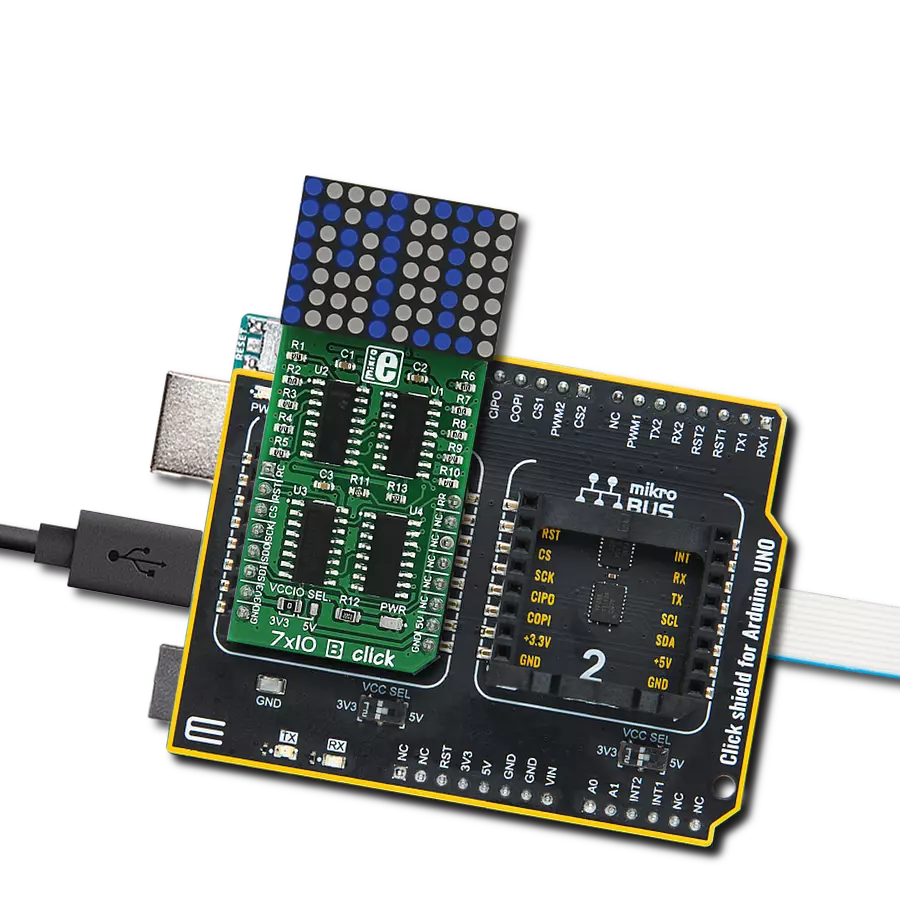
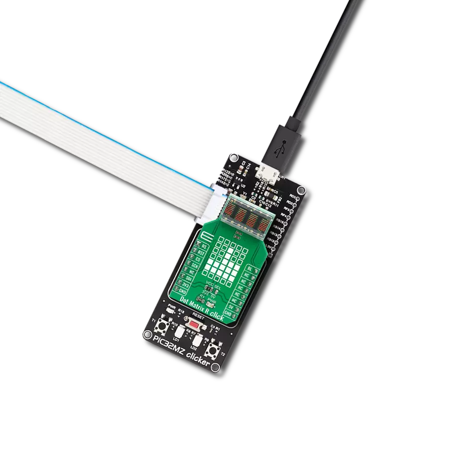
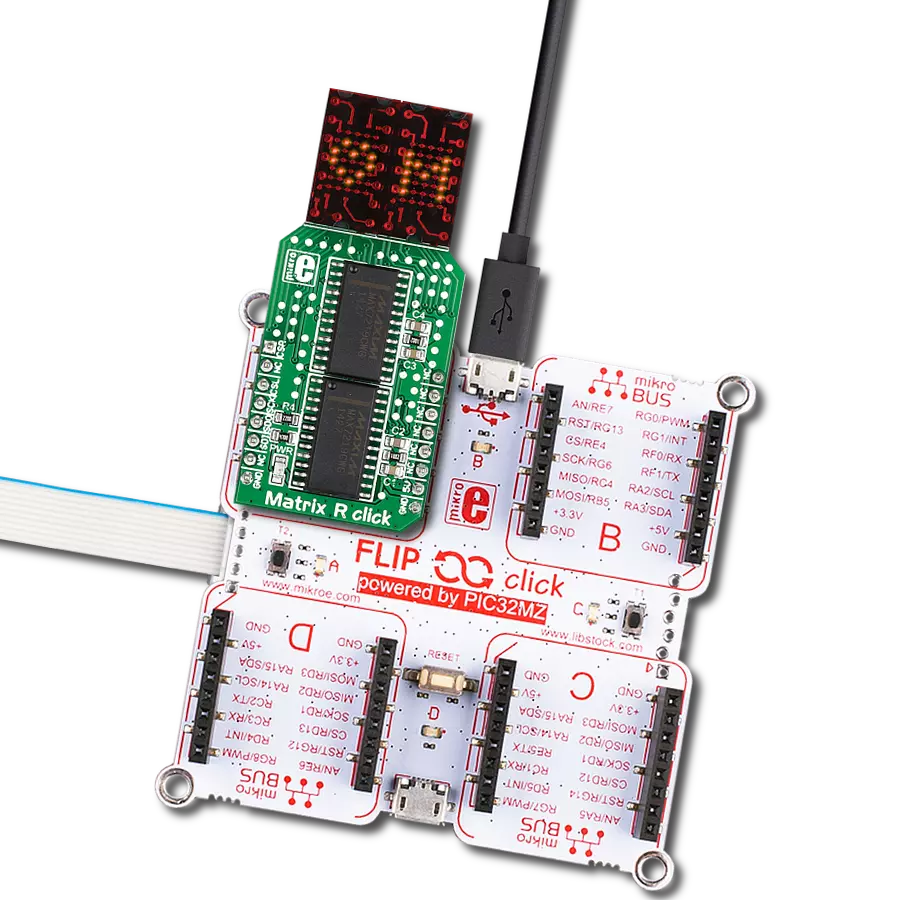
7x10 B Click
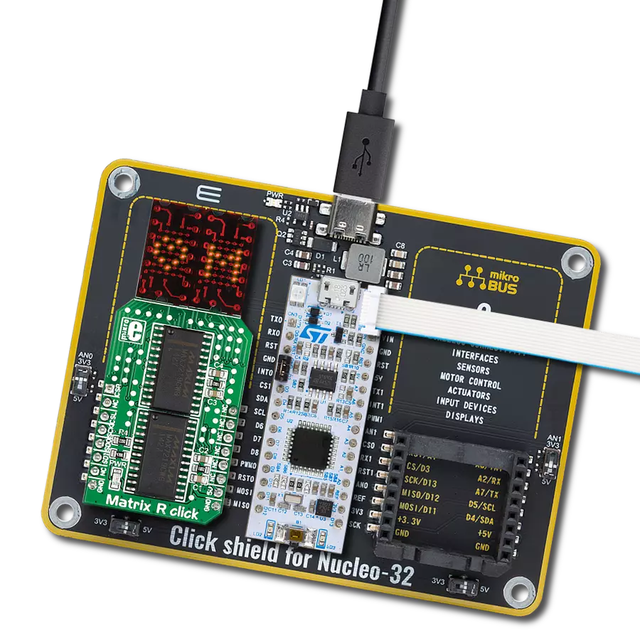
Dev. board
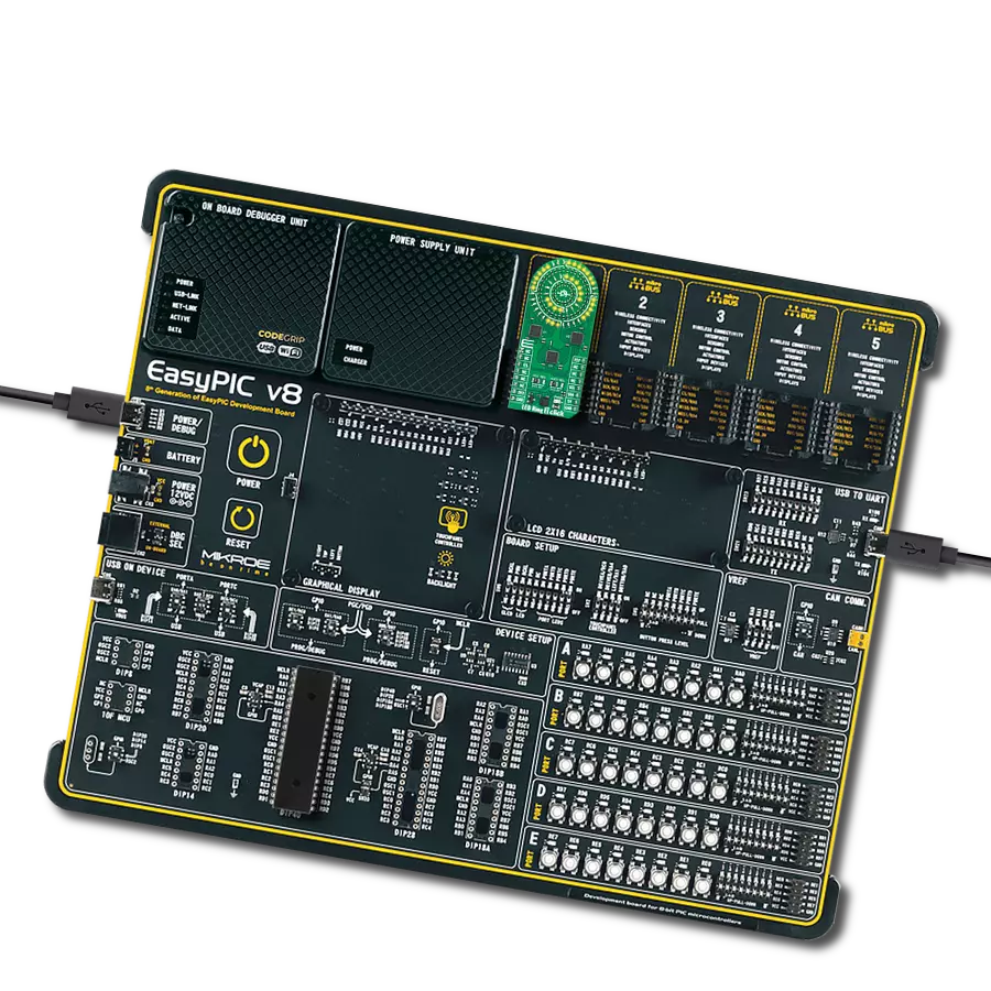
UNI-DS v8
Compiler
NECTO Studio
MCU
PIC18F86J55
Experience the vividness of our 7x10 green LED display, designed to captivate and engage your audience with bright and eco-friendly visuals, perfect for signage, notifications, and creative projects
A
A
Hardware Overview
How does it work?
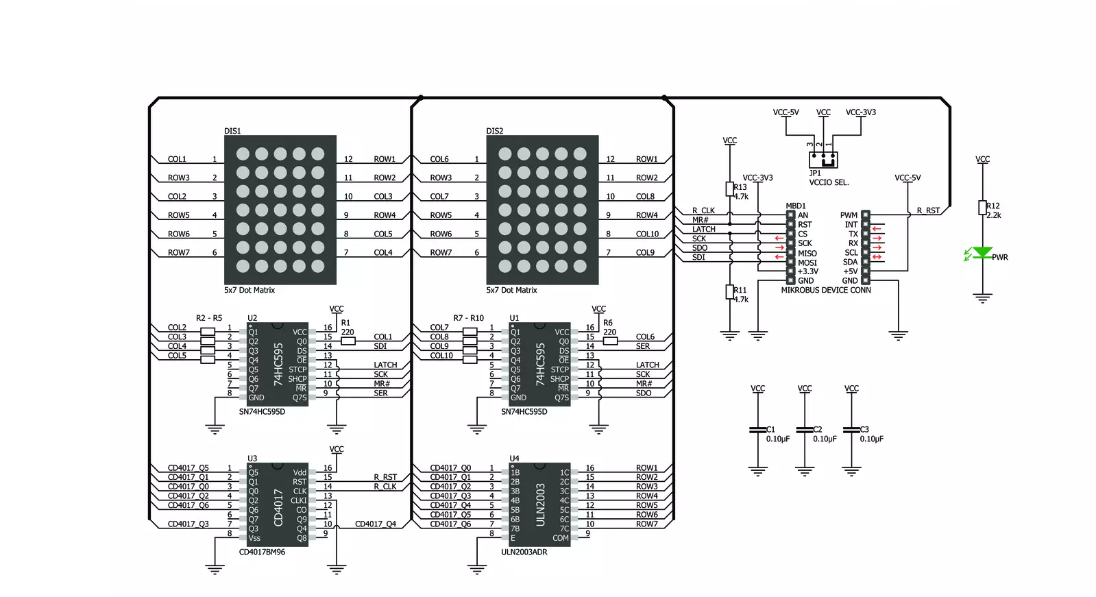
7x10 B Click is an LED dot matrix display click, which can be used to display graphics or letters very easily. The click board has two LED dot matrix modules with 7x5 stylish, round, dot-like LED elements. These displays produce clean and uniform patterns since the elements are optically isolated from each other, and there is no light bleeding between the adjacent LED cells. Additionally, turn-on and turn-off times of the matrix cells are optimized for a clean and fluid display performance, with no flickering or lag. This click board™ can be used in a lot of different applications that require a clearly visible display of text or graphics, such as the public clock displays, temperature displays and similar. By using functions provided by MIKROE, it is possible to make a text scroller in a very simple way, greatly expanding the functionality of the 7x10 click. Two 7x5 LED dot matrix modules form a display. A single LED matrix module is composed of 35 LED elements, grouped in rows and columns. The LED elements in one row have their cathodes connected and routed to a single row pin. The LED elements in one column have their anodes connected and routed to a single column pin. Multiplexed like this, modules have a fairly low number of pins (12 per module), making them suitable to be driven by shift registers and a decade counter ICs. The driver circuit consists of two 74HC595 - 8bit, serial input - parallel output shift registers, one CD4017 - a Jonson topology decade counter with 10 outputs, and one ULN2003A - an IC with seven integrated Darlington transistor pairs, all chips produced by Texas Instruments. The device communicates with the host MCU via the SPI interface. Two 8bit words of information are pushed through the serial data input pin of the first 74HC595 shift register IC.
Since there are 5 columns on one module, both of these bytes must have their three MSB set to 0. Two shift register ICs (SR) are connected so that the serial data output of the first SR is connected to the serial data input of the second SR. When more than 8 bits are clocked in the first SR, they will start pushing (shifting) the bits serially into the second SR. After both of the internal storage registers of the SRs are loaded with the data this way, the SPI communication should be terminated (SCK signal stopped) and the rising edge of the LATCH pin (routed to mikroBUS™ CS pin) will cause the stored data to appear on the output pins of two SRs, in parallel form. This will not light up the corresponding LED elements yet; it will only polarize their anodes. To complete LEDs current path, their cathodes must be connected to ground. This is where the CD4017 and ULN2003 ICs are used. The ULN2003 IC is used to drive rows of the dot matrix displays, by sinking the current on the active row. When there is no signal at the low-current side inputs of the ULN2003 IC, its outputs will be in a high impedance mode (High-Z), causing the inactive rows to be disconnected and their current path - obstructed. None of the LED elements on a disconnected row will be able to light up, even if their anodes were polarized by the SRs. To activate one of the 7 input channels of the ULN2003 IC, the CD4017 decade counter IC is used. It is perfect for this task since it will shift forward its active output for one position, with every clock pulse. Again, since this is a decade counter (10 outputs), only first 7 channels are used. To skip last 3 cycles, the counter IC needs to be reset, by means of the RST pin, routed to the RST pin of the mikroBUS™. When the specific row is activated, LEDs on that row, which have their anodes polarized by the SRs, will be lit - since the
current will be able to sink through the Darlington pairs to the ground. This is how the multiplication is implemented. The design of the decade counter allows only one row to be active at a time. So, in order to see the complete picture on a led matrix, the row scanning has to be fast enough, so that the effect called persistent vision takes place. It produces an illusion of a complete image, even if only one row is seen at a time - because the human eye is not able to detect very fast changes of light. Scanline method is a very old method for displaying a picture on a number of various displays - starting with old CRT displays, up to modern TFT computer screens. However, for this effect to work, the timing is very important. To switch to the next row, the data on the previous row needs to be displayed first. Therefore, the clock impulse for the CD4017 needs to occur after all the 16 bits from the SPI bus were clocked in the SRs and latched out to LED elements, plus a small delay to allow the line to be absorbed by the human eye. Therefore, the R_CLK clock pin of the CD4017 is routed to the AN pin of the mikroBUS™. The #MR pin is used to clear the data in the internal storage register of the ICs. The LOW logic level on this pin will clear the content of this register but will not turn off the outputs already activated. The #MR pin is routed to the RST pin of the mikroBUS™ and it is pulled to a HIGH logic level by the onboard resistor. This Click board™ can operate with either 3.3V or 5V logic voltage levels selected via the VCC SEL jumper. This way, both 3.3V and 5V capable MCUs can use the communication lines properly. Also, this Click board™ comes equipped with a library containing easy-to-use functions and an example code that can be used as a reference for further development.


Features overview
Development board
UNI-DS v8 is a development board specially designed for the needs of rapid development of embedded applications. It supports a wide range of microcontrollers, such as different STM32, Kinetis, TIVA, CEC, MSP, PIC, dsPIC, PIC32, and AVR MCUs regardless of their number of pins, and a broad set of unique functions, such as the first-ever embedded debugger/programmer over WiFi. The development board is well organized and designed so that the end-user has all the necessary elements, such as switches, buttons, indicators, connectors, and others, in one place. Thanks to innovative manufacturing technology, UNI-DS v8 provides a fluid and immersive working experience, allowing access anywhere and under any
circumstances at any time. Each part of the UNI-DS v8 development board contains the components necessary for the most efficient operation of the same board. An advanced integrated CODEGRIP programmer/debugger module offers many valuable programming/debugging options, including support for JTAG, SWD, and SWO Trace (Single Wire Output)), and seamless integration with the Mikroe software environment. Besides, it also includes a clean and regulated power supply module for the development board. It can use a wide range of external power sources, including a battery, an external 12V power supply, and a power source via the USB Type-C (USB-C) connector. Communication options such as USB-UART, USB
HOST/DEVICE, CAN (on the MCU card, if supported), and Ethernet is also included. In addition, it also has the well-established mikroBUS™ standard, a standardized socket for the MCU card (SiBRAIN standard), and two display options for the TFT board line of products and character-based LCD. UNI-DS v8 is an integral part of the Mikroe ecosystem for rapid development. Natively supported by Mikroe software tools, it covers many aspects of prototyping and development thanks to a considerable number of different Click boards™ (over a thousand boards), the number of which is growing every day.

Microcontroller Overview
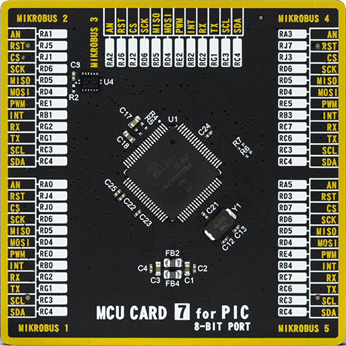
MCU Card / MCU
Type
8th Generation
Architecture
PIC
MCU Memory (KB)
96
Silicon Vendor
Microchip
Pin count
80
RAM (Bytes)
3904
Used MCU Pins
mikroBUS™ mapper
Take a closer look
Click board™ Schematic
Step by step
Project assembly

Start by selecting your development board and Click board™. Begin with the UNI-DS v8 as your development board.


Software Support
Library Description
This library contains API for 7x10 B Click driver.
Key functions:
c7x10b_draw_pixel- Drawing the pixel on the displayc7x10b_draw_char- Drawing the character on the displayc7x10b_draw_number- Drawing the number on the display
Open Source
Code example
The complete application code and a ready-to-use project are available through the NECTO Studio Package Manager for direct installation in the NECTO Studio. The application code can also be found on the MIKROE GitHub account.
/*!
 * @file main.c
 * @brief c7x10B Click example
 *
 * # Description
 * This demo example shows a drawing of pixels, characters and a number on the screen.
 *
 * The demo application is composed of two sections :
 *
 * ## Application Init
 * Configuring the Click board.
 *
 * ## Application Task
 * Draws characters, numbers, and pixels to the display.
 *
 * @author Jelena Milosavljevic
 *
 */
// ------------------------------------------------------------------- INCLUDES

#include "board.h"
#include "c7x10b.h"

// ------------------------------------------------------------------ VARIABLES

static c7x10b_t c7x10b;

// ------------------------------------------------------ APPLICATION FUNCTIONS

void application_init ( void ) {

   c7x10b_cfg_t c7x10b_cfg;  /**< Click config object. */

    //  Click initialization.

    c7x10b_cfg_setup( &c7x10b_cfg );
    C7X10B_MAP_MIKROBUS( c7x10b_cfg, MIKROBUS_1 );
    c7x10b_init( &c7x10b, &c7x10b_cfg );
}

void application_task ( void ) {

    c7x10b_pixel_t pixel;
    uint8_t cnt;
    uint8_t cnt_x;
    uint8_t cnt_y;

    // CHAR PROCEDURE

    for ( cnt = 'A'; cnt < 'Z'; cnt+=2 ) {

        c7x10b_draw_char( &c7x10b, cnt, C7X10B_DISPLAY_LEFT, C7X10B_DISPLAY_DELAY_50MS );
        c7x10b_draw_char( &c7x10b, cnt + 1, C7X10B_DISPLAY_RIGHT | C7X10B_DISPLAY_REFRESH, C7X10B_DISPLAY_DELAY_50MS );

        Delay_ms ( 1000 );
    }

    // COUNTER PROCEDURE

    for ( cnt = 0; cnt < 15; cnt++ ) {

        c7x10b_draw_number( &c7x10b, cnt, C7X10B_DISPLAY_DELAY_50MS );

        Delay_ms ( 500 );
    }

    // PIXELS PROCEDURE

    for ( cnt_x = 0; cnt_x <= 7; cnt_x++ ) {

        for ( cnt_y = 0; cnt_y <= 10; cnt_y++ ) {

            pixel.cord_x = cnt_x;
            pixel.cord_y = cnt_y;
            c7x10b_draw_pixel( &c7x10b, &pixel, C7X10B_DISPLAY_PIXEL_STORAGE,
                                              C7X10B_DISPLAY_DELAY_20MS );

            pixel.cord_x = cnt_x;
            pixel.cord_y = cnt_y + 1;
            c7x10b_draw_pixel( &c7x10b, &pixel, C7X10B_DISPLAY_PIXEL_REFRESH,
                                              C7X10B_DISPLAY_DELAY_20MS );
        }
    }
}

int main ( void )
{
    /* Do not remove this line or clock might not be set correctly. */
    #ifdef PREINIT_SUPPORTED
    preinit();
    #endif

    application_init( );

    for ( ; ; )
    {
        application_task( );
    }

    return 0;
}

// ------------------------------------------------------------------------ END
Additional Support
Resources
Category:LED Matrix