Make accurate digital representation of analog signals with ADC121S021 and MK64FN1M0VDC12
Embrace the digital age

Published Jun 08, 2023
Click board™
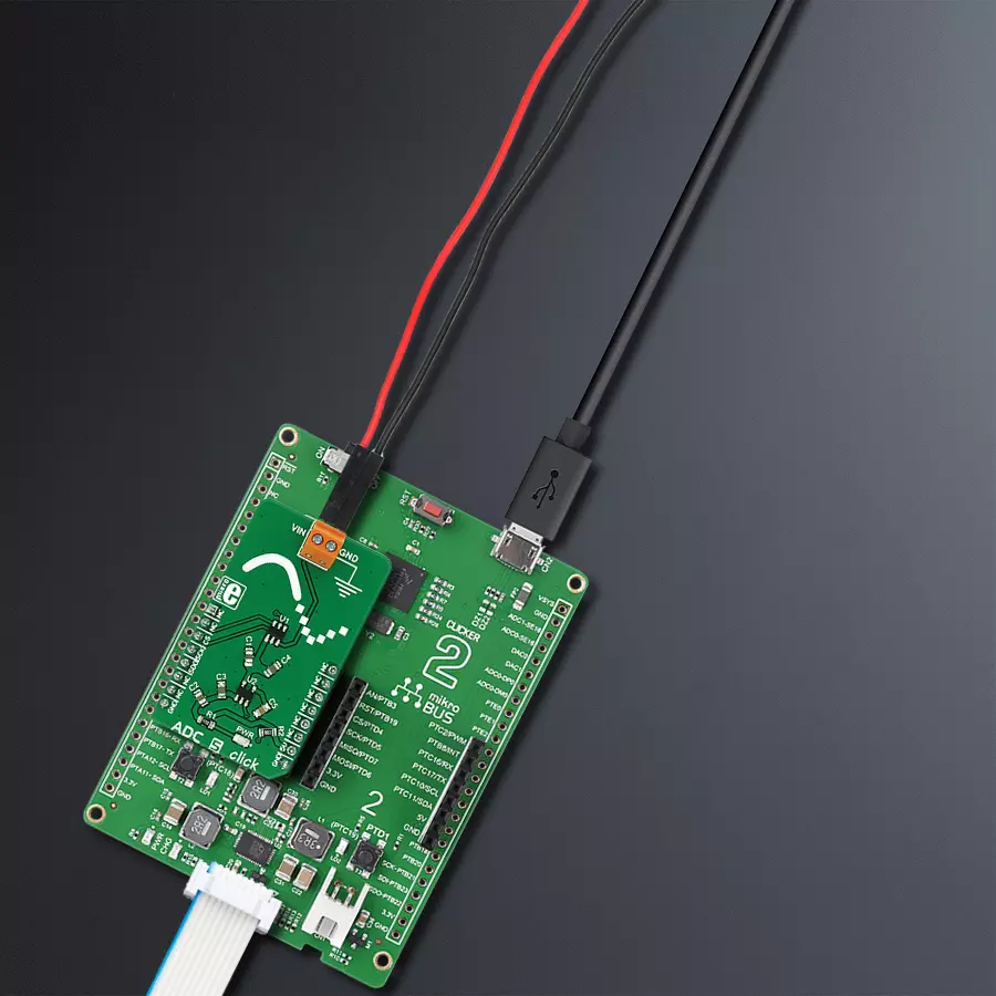
ADC 5 click
Dev. board
Clicker 2 for Kinetis
Compiler
NECTO Studio
MCU
MK64FN1M0VDC12
Don't settle for less than the best – choose our ADC for your next project!
A
A
Hardware Overview
How does it work?
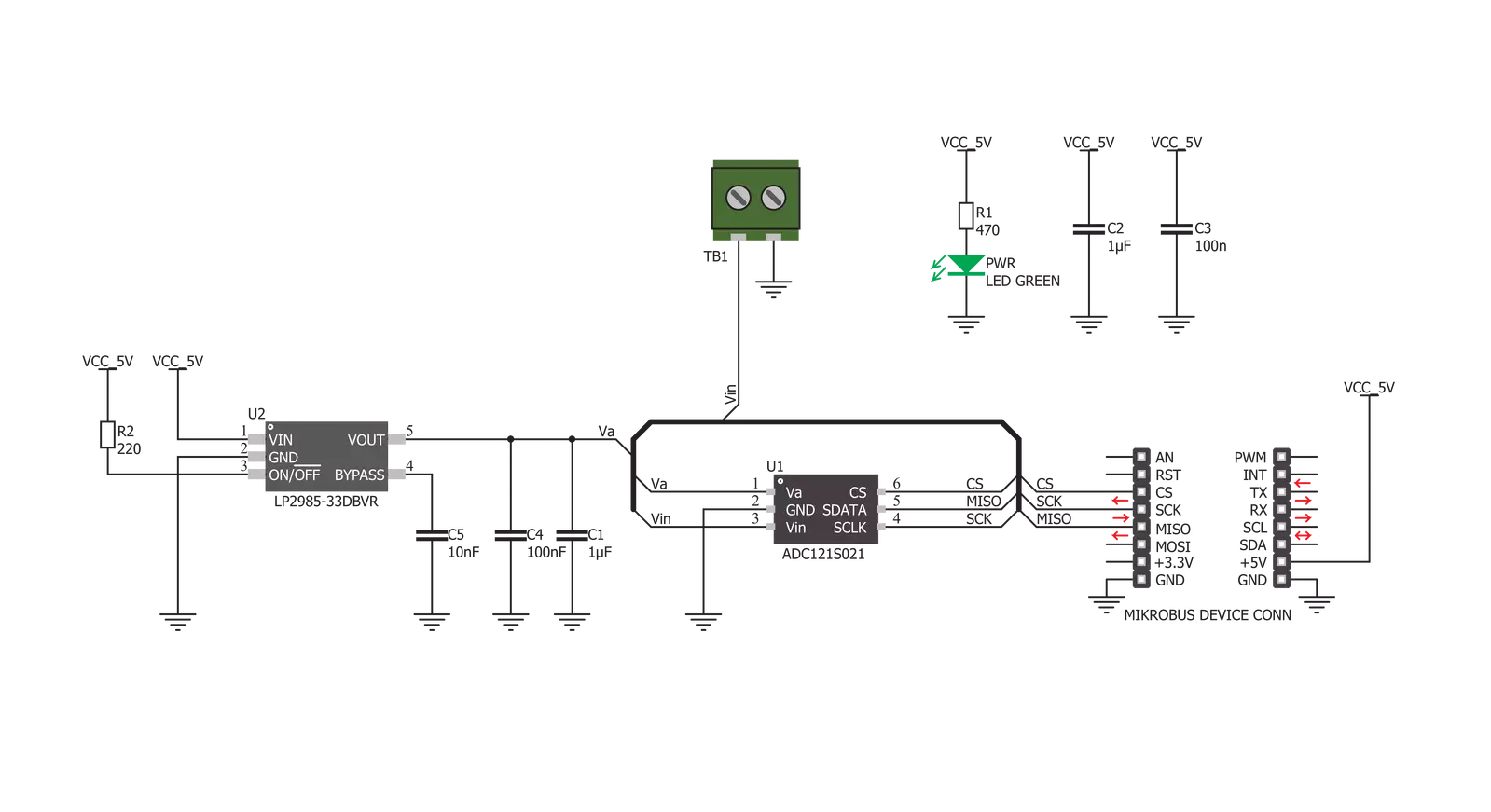
ADC 5 Click is based on the ADC121S021, a 12-bit CMOS ADC device from Texas Instruments. This AD converter uses a reference voltage obtained from the LP2985 LDO regulator from the same company. It provides a clean and accurate regulated voltage on its output, perfectly suited to this converter's reference voltage. Since the reference voltage is set to 3.3V, the maximum value of the input voltage is also 3.3V. The device uses SPI communication. The MOSI pin does not exist since no communication from the MCU to the click board™ is going on. The reading speed, also known as the sample rate, directly depends on the clock rate of the SCK line. The sample rate over which the specified electrical performance is ensured is 50 Ks/s to 200 Ks/s. The ADC121S021 can use any clock signal frequency up to the rated maximum frequency, with
no significant deviations from the specifications stated in the datasheet: it is specified over a wide range of sample rates, maintaining good linearity and high signal-to-noise ratio (SNR). ADC (analog to digital converters) are the most commonly used devices for converting voltage signals into information, which can then be processed in the digital domain. There are many types of ADC converters commercially available. They can vary in bit depth, sample rate, approximation algorithm (SAR or delta-sigma), and more. Those attributes affect how accurately the sampled voltage will be translated into the digital world. The sample rate is usually the determining factor when the maximum frequency of the input signal is considered. The aliasing of the input signal can occur as the input signal frequency is nearing half the sample rate
of the converter. This frequency limits the bandwidth of the input signal, also called the Nyquist frequency, so using input frequencies near or above the Nyquist frequency results in an inaccurate conversion. The ADC121S021 converter uses the SAR, or the successive approximation method, for the conversion, which compares the input voltage with a series of internally generated voltage values. The approximation is stored in a successive approximation register at each step in this process. The comparing steps are continued until the desired resolution is reached. The ADC click board is also equipped with a screw terminal, which can be used for easy and secure connection of the input voltage rail. Although the reference voltage is 3.3V, it is powered only by the 5V rail from the mikroBUS™, used as the input for the LDO regulator.

Features overview
Development board
Clicker 2 for Kinetis is a compact starter development board that brings the flexibility of add-on Click boards™ to your favorite microcontroller, making it a perfect starter kit for implementing your ideas. It comes with an onboard 32-bit ARM Cortex-M4F microcontroller, the MK64FN1M0VDC12 from NXP Semiconductors, two mikroBUS™ sockets for Click board™ connectivity, a USB connector, LED indicators, buttons, a JTAG programmer connector, and two 26-pin headers for interfacing with external electronics. Its compact design with clear and easily recognizable silkscreen markings allows you to build gadgets with unique functionalities and
features quickly. Each part of the Clicker 2 for Kinetis development kit contains the components necessary for the most efficient operation of the same board. In addition to the possibility of choosing the Clicker 2 for Kinetis programming method, using a USB HID mikroBootloader or an external mikroProg connector for Kinetis programmer, the Clicker 2 board also includes a clean and regulated power supply module for the development kit. It provides two ways of board-powering; through the USB Micro-B cable, where onboard voltage regulators provide the appropriate voltage levels to each component on the board, or
using a Li-Polymer battery via an onboard battery connector. All communication methods that mikroBUS™ itself supports are on this board, including the well-established mikroBUS™ socket, reset button, and several user-configurable buttons and LED indicators. Clicker 2 for Kinetis is an integral part of the Mikroe ecosystem, allowing you to create a new application in minutes. Natively supported by Mikroe software tools, it covers many aspects of prototyping thanks to a considerable number of different Click boards™ (over a thousand boards), the number of which is growing every day.

Microcontroller Overview
MCU Card / MCU

Architecture
ARM Cortex-M4
MCU Memory (KB)
1024
Silicon Vendor
NXP
Pin count
121
RAM (Bytes)
262144
Used MCU Pins
mikroBUS™ mapper
Take a closer look
Click board™ Schematic
Step by step
Project assembly

Start by selecting your development board and Click board™. Begin with the Clicker 2 for Kinetis as your development board.


Software Support
Library Description
This library contains API for ADC 5 Click driver.
Key functions:
adc5_getData - This function returns raw 10-bit data
adc5_getVoltage - This function returns measured voltage in millivolts
Open Source
Code example
The complete application code and a ready-to-use project are available through the NECTO Studio Package Manager for direct installation in the NECTO Studio. The application code can also be found on the MIKROE GitHub account.
/*!
 * \file
 * \brief ADC5 Click example
 *
 * # Description
 * This example showcases how to initialize and configure the logger and Click modules and
 * how to read and display ADC voltage data from the Click.
 *
 * The demo application is composed of two sections :
 *
 * ## Application Init
 * This function initializes and configures the logger and Click modules.
 *
 * ## Application Task
 * This function reads and displays ADC voltage data every second.
 *
 * \author MikroE Team
 *
 */
// ------------------------------------------------------------------- INCLUDES

#include "board.h"
#include "log.h"
#include "adc5.h"

// ------------------------------------------------------------------ VARIABLES

static adc5_t adc5;
static log_t logger;

// ------------------------------------------------------ APPLICATION FUNCTIONS

void application_init ( )
{
    log_cfg_t log_cfg;
    adc5_cfg_t cfg;

    /**
     * Logger initialization.
     * Default baud rate: 115200
     * Default log level: LOG_LEVEL_DEBUG
     * @note If USB_UART_RX and USB_UART_TX
     * are defined as HAL_PIN_NC, you will
     * need to define them manually for log to work.
     * See @b LOG_MAP_USB_UART macro definition for detailed explanation.
     */
    LOG_MAP_USB_UART( log_cfg );
    log_init( &logger, &log_cfg );
    log_info( &logger, "---- Application Init ----" );
    Delay_ms ( 100 );

    //  Click initialization.

    adc5_cfg_setup( &cfg );
    ADC5_MAP_MIKROBUS( cfg, MIKROBUS_1 );
    adc5_init( &adc5, &cfg );
}

void application_task ( )
{
    uint16_t adc_value;

    adc_value = adc5_get_voltage( &adc5 );
    log_printf( &logger, " * Voltage: %d mV * \r\n", adc_value );
    Delay_1sec( );
}

int main ( void )
{
    /* Do not remove this line or clock might not be set correctly. */
    #ifdef PREINIT_SUPPORTED
    preinit();
    #endif

    application_init( );

    for ( ; ; )
    {
        application_task( );
    }

    return 0;
}

// ------------------------------------------------------------------------ END


