Transform your data storage experience with EM064LX and MK64FN1M0VDC12
Our MRAM memory, your data's secure haven.

Published Nov 14, 2023
Click board™
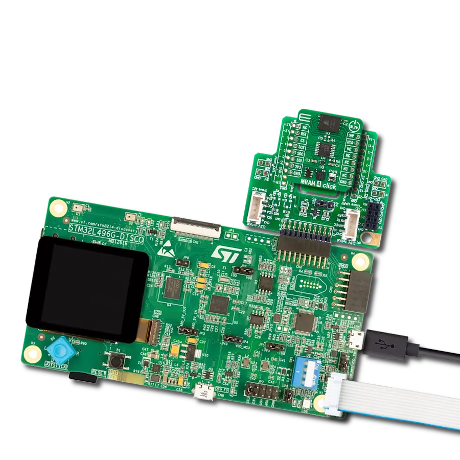
MRAM 4 Click
Dev. board
Clicker 2 for Kinetis
Compiler
NECTO Studio
MCU
MK64FN1M0VDC12
Our MRAM memory solution sets a new standard in data storage technology, combining rapid access speeds with magnetic reliability for a seamless and efficient user experience.
A
A
Hardware Overview
How does it work?
MRAM 4 Click is based on the EM064LX, an industrial STT-MRAM persistent memory from Everspin Technologies. It can deliver up to 400Mbps reads and writes via eight I/O signals with a clock frequency of 200MHz. As this is a persistent memory, byte-level writes and reads do not require erasing. Nonvolatile settings are not reflow protected, which you have to keep in mind. A dedicated 256-byte OTP area outside the main memory is readable and user-lockable, with a permanent lock WRITE OTP command. The EM064LX is capable of chip/bulk and sector erase. Subsector erase is possible in 4KB, 32KB granularity. In addition, the MRAM memory features 16 configurable hardware write-protected
regions plus top/bottom select, program/erase protection during power-up, and CRC command to detect accidental changes to user data. As the EM064LX works at the recommended 1.8V voltage, the MRAM 4 Click is equipped with a BH18PB1WHFV, a CMOS LDO regulator from Rohm Semiconductor. To work with different logic level voltage, this Click board™ comes with a TXB0106, a 6-bit bidirectional level-shifting and voltage translator from Texas Instruments. On board, there are two unpopulated jumpers labeled R5 and R6. The chip select and write protection can be pulled up for further hardware development. MRAM 4 Click uses a standard 4-Wire SPI serial interface to communicate
with the host MCU. You can use write protection functionality over the WP pin. The hardware reset is available over the HLD pin, whereas in the low logic state, the memory will self-initialize and return the device to the ready state. There is an unpopulated R6 resistor for an external pull-up, as this pin shouldn’t be allowed to float. This Click board™ can be operated only with a 3.3V logic voltage level. The board must perform appropriate logic voltage level conversion before using MCUs with different logic levels. Also, it comes equipped with a library containing functions and an example code that can be used as a reference for further development.

Features overview
Development board
Clicker 2 for Kinetis is a compact starter development board that brings the flexibility of add-on Click boards™ to your favorite microcontroller, making it a perfect starter kit for implementing your ideas. It comes with an onboard 32-bit ARM Cortex-M4F microcontroller, the MK64FN1M0VDC12 from NXP Semiconductors, two mikroBUS™ sockets for Click board™ connectivity, a USB connector, LED indicators, buttons, a JTAG programmer connector, and two 26-pin headers for interfacing with external electronics. Its compact design with clear and easily recognizable silkscreen markings allows you to build gadgets with unique functionalities and
features quickly. Each part of the Clicker 2 for Kinetis development kit contains the components necessary for the most efficient operation of the same board. In addition to the possibility of choosing the Clicker 2 for Kinetis programming method, using a USB HID mikroBootloader or an external mikroProg connector for Kinetis programmer, the Clicker 2 board also includes a clean and regulated power supply module for the development kit. It provides two ways of board-powering; through the USB Micro-B cable, where onboard voltage regulators provide the appropriate voltage levels to each component on the board, or
using a Li-Polymer battery via an onboard battery connector. All communication methods that mikroBUS™ itself supports are on this board, including the well-established mikroBUS™ socket, reset button, and several user-configurable buttons and LED indicators. Clicker 2 for Kinetis is an integral part of the Mikroe ecosystem, allowing you to create a new application in minutes. Natively supported by Mikroe software tools, it covers many aspects of prototyping thanks to a considerable number of different Click boards™ (over a thousand boards), the number of which is growing every day.

Microcontroller Overview
MCU Card / MCU

Architecture
ARM Cortex-M4
MCU Memory (KB)
1024
Silicon Vendor
NXP
Pin count
121
RAM (Bytes)
262144
Used MCU Pins
mikroBUS™ mapper
Take a closer look
Click board™ Schematic

Step by step
Project assembly

Start by selecting your development board and Click board™. Begin with the Clicker 2 for Kinetis as your development board.


Track your results in real time
Application Output
1. Application Output - In Debug mode, the 'Application Output' window enables real-time data monitoring, offering direct insight into execution results. Ensure proper data display by configuring the environment correctly using the provided tutorial.

2. UART Terminal - Use the UART Terminal to monitor data transmission via a USB to UART converter, allowing direct communication between the Click board™ and your development system. Configure the baud rate and other serial settings according to your project's requirements to ensure proper functionality. For step-by-step setup instructions, refer to the provided tutorial.

3. Plot Output - The Plot feature offers a powerful way to visualize real-time sensor data, enabling trend analysis, debugging, and comparison of multiple data points. To set it up correctly, follow the provided tutorial, which includes a step-by-step example of using the Plot feature to display Click board™ readings. To use the Plot feature in your code, use the function: plot(*insert_graph_name*, variable_name);. This is a general format, and it is up to the user to replace 'insert_graph_name' with the actual graph name and 'variable_name' with the parameter to be displayed.

Software Support
Library Description
This library contains API for MRAM 4 Click driver.
Key functions:
mram4_memory_write- MRAM 4 memory write function.mram4_memory_read- MRAM 4 memory read function.mram4_block_erase- MRAM 4 block erase function.
Open Source
Code example
The complete application code and a ready-to-use project are available through the NECTO Studio Package Manager for direct installation in the NECTO Studio. The application code can also be found on the MIKROE GitHub account.
/*!
 * @file main.c
 * @brief MRAM 4 Click example
 *
 * # Description
 * This example demonstrates the use of MRAM 4 Click board.
 * The demo app writes specified data to the memory and reads it back.
 *
 * The demo application is composed of two sections :
 *
 * ## Application Init
 * The initialization of SPI module, log UART, and additional pins.
 * After the driver init, the app executes a default configuration.
 *
 * ## Application Task
 * The demo application writes a desired number of bytes to the memory
 * and then verifies if it is written correctly
 * by reading from the same memory location and displaying the memory content.
 * Results are being sent to the UART Terminal, where you can track their changes.
 *
 * @author Nenad Filipovic
 *
 */

#include "board.h"
#include "log.h"
#include "mram4.h"

static mram4_t mram4;
static log_t logger;

#define STARTING_ADDRESS             0x012345ul
#define DEMO_TEXT_MESSAGE_1         "MikroE"
#define DEMO_TEXT_MESSAGE_2         "MRAM 4 Click"

void application_init ( void )
{
    log_cfg_t log_cfg;  /**< Logger config object. */
    mram4_cfg_t mram4_cfg;  /**< Click config object. */

    /**
     * Logger initialization.
     * Default baud rate: 115200
     * Default log level: LOG_LEVEL_DEBUG
     * @note If USB_UART_RX and USB_UART_TX
     * are defined as HAL_PIN_NC, you will
     * need to define them manually for log to work.
     * See @b LOG_MAP_USB_UART macro definition for detailed explanation.
     */
    LOG_MAP_USB_UART( log_cfg );
    log_init( &logger, &log_cfg );
    log_info( &logger, " Application Init " );

    // Click initialization.
    mram4_cfg_setup( &mram4_cfg );
    MRAM4_MAP_MIKROBUS( mram4_cfg, MIKROBUS_1 );
    if ( SPI_MASTER_ERROR == mram4_init( &mram4, &mram4_cfg ) )
    {
        log_error( &logger, " Communication init." );
        for ( ; ; );
    }

    if ( MRAM4_ERROR == mram4_default_cfg ( &mram4 ) )
    {
        log_error( &logger, " Default configuration." );
        for ( ; ; );
    }
    Delay_ms ( 100 );

    log_info( &logger, " Application Task " );
    log_printf( &logger, "-----------------------\r\n" );
    Delay_ms ( 100 );
}

void application_task ( void )
{
    uint8_t data_buf[ 128 ] = { 0 };
    log_printf( &logger, " Memory address: 0x%.6LX\r\n", ( uint32_t ) STARTING_ADDRESS );
    if ( MRAM4_OK == mram4_block_erase( &mram4, MRAM4_CMD_ERASE_4KB, STARTING_ADDRESS ) )
    {
        log_printf( &logger, " Erase memory block (4KB)\r\n" );
        Delay_ms ( 100 );
    }

    memcpy( data_buf, DEMO_TEXT_MESSAGE_1, strlen( DEMO_TEXT_MESSAGE_1 ) );
    if ( MRAM4_OK == mram4_memory_write( &mram4, STARTING_ADDRESS, data_buf, sizeof( data_buf ) ) )
    {
        log_printf( &logger, " Write data: %s\r\n", data_buf );
        Delay_ms ( 100 );
    }

    memset( data_buf, 0, sizeof( data_buf ) );
    if ( MRAM4_OK == mram4_memory_read( &mram4, STARTING_ADDRESS, data_buf, sizeof( data_buf ) ) )
    {
        log_printf( &logger, " Read data: %s\r\n", data_buf );
        Delay_ms ( 1000 );
        Delay_ms ( 1000 );
        Delay_ms ( 1000 );
    }
    log_printf( &logger, " ----------------------------\r\n" );

    log_printf( &logger, " Memory address: 0x%.6LX\r\n", ( uint32_t ) STARTING_ADDRESS );
    if ( MRAM4_OK == mram4_block_erase( &mram4, MRAM4_CMD_ERASE_4KB, STARTING_ADDRESS ) )
    {
        log_printf( &logger, " Erase memory block (4KB)\r\n" );
    }

    memcpy( data_buf, DEMO_TEXT_MESSAGE_2, strlen( DEMO_TEXT_MESSAGE_2 ) );
    if ( MRAM4_OK == mram4_memory_write( &mram4, STARTING_ADDRESS, data_buf, sizeof( data_buf ) ) )
    {
        log_printf( &logger, " Write data: %s\r\n", data_buf );
        Delay_ms ( 100 );
    }

    memset( data_buf, 0, sizeof( data_buf ) );
    if ( MRAM4_OK == mram4_memory_read( &mram4, STARTING_ADDRESS, data_buf, sizeof( data_buf ) ) )
    {
        log_printf( &logger, " Read data: %s\r\n", data_buf );
        Delay_ms ( 1000 );
        Delay_ms ( 1000 );
        Delay_ms ( 1000 );
    }
    log_printf ( &logger, " ----------------------------\r\n" );
}

int main ( void )
{
    /* Do not remove this line or clock might not be set correctly. */
    #ifdef PREINIT_SUPPORTED
    preinit();
    #endif

    application_init( );

    for ( ; ; )
    {
        application_task( );
    }

    return 0;
}

// ------------------------------------------------------------------------ END