Upgrade your data presentation with SMA-B500LE and PIC18F4515
Data insights, one segment at a time!
Published Nov 01, 2023
Click board™
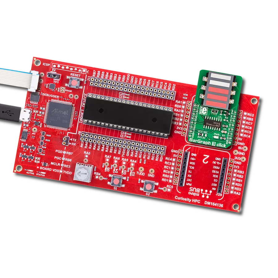
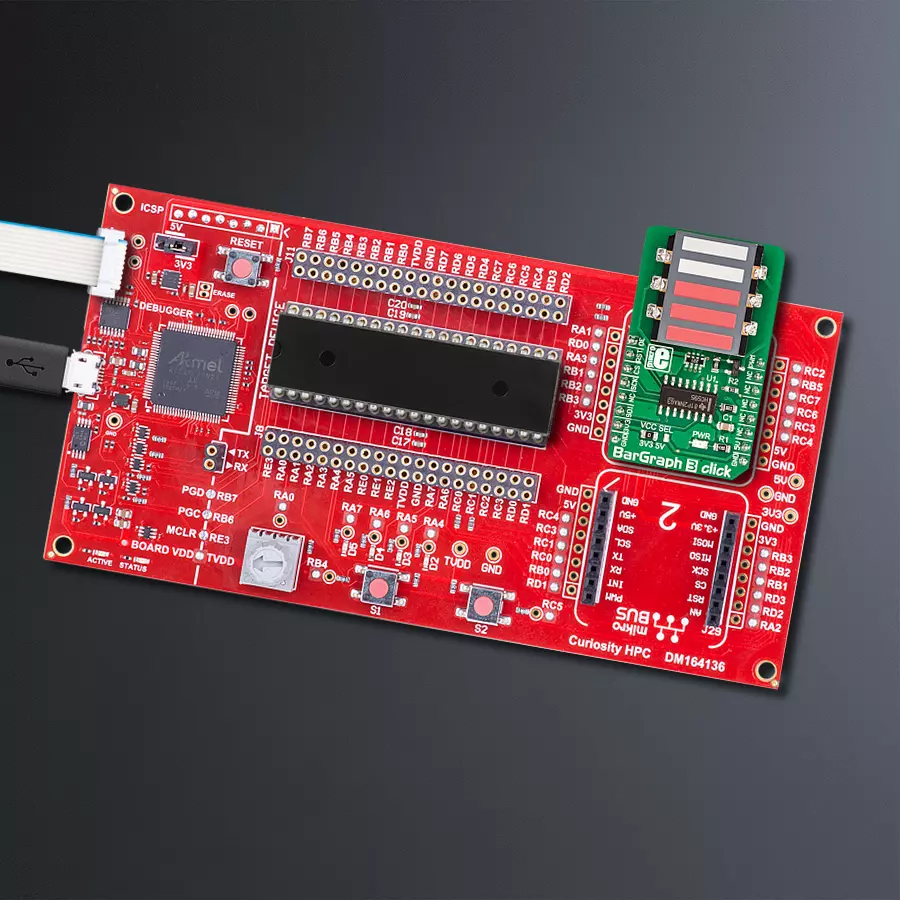
BarGraph 3 Click
Dev. board
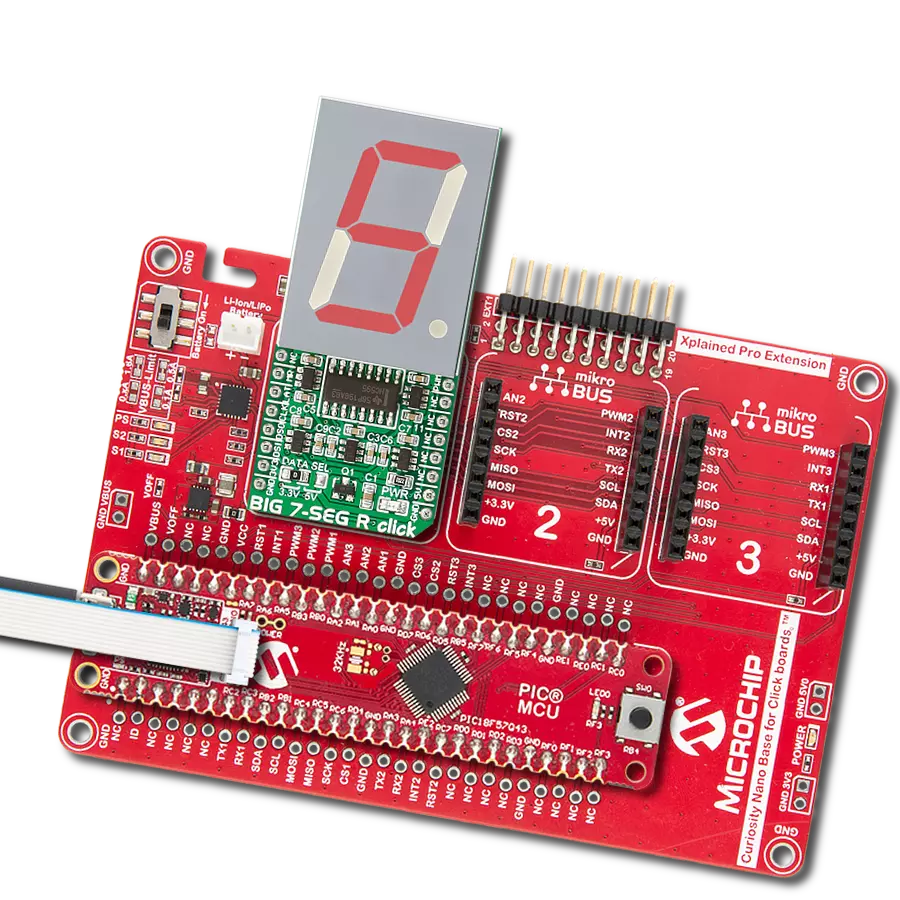
Curiosity HPC
Compiler
NECTO Studio
MCU
PIC18F4515
Our 5-segment red bar graph display is designed to provide a straightforward and precise way to visualize data, making it ideal for various applications where simplicity and clarity are essential
A
A
Hardware Overview
How does it work?
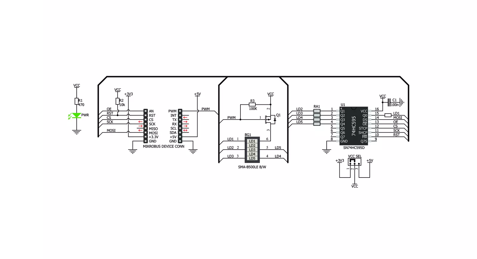
BarGraph 3 Click is equipped with a five-segment LED bar graph display, notable for its strong and uniform illumination of the segments. When it comes to driving an array of LED segments, using so-called shift-register ICs is almost unavoidable. This Click board™ uses a single 74HC595 IC, a tri-state, serial-in, parallel-out, 8-bit shift-register with output latch, from Texas Instruments. It is used to drive the SMA-B500LE a monochrome (red) 5 segment bar graph array, from American Opto Plus LED corporation. The 74HC595 ICs is comprised of a D-type internal storage register, and a serial-to-parallel shift register, both 8 bits wide. Each of these registers has its own clock line, making it possible to clock in the desired data in, and then clock it out to the parallel output pins when needed. The SMA-B500LE bar graph LED array has 5 red LED segments. Each segment contains three LEDs, with their cathodes connected in a single point and routed out as the single common cathode pin. This results with a bar graph display that has only six pins, even though it uses 15 LED elements in total. Similarly, all the anodes of the LED segments are routed to a single pin, which is connected to the drain of the P channel MOSFET, while its source is connected to the VCC. Driving the gate of the MOSFET using the PWM pin of the mikroBUS™ allows dimming of the LED bar graph display, by changing the pulse
width of the applied PWM signal. The Click board™ communicates with the host MCU over the SPI interface, routed to the mikroBUS™ MOSI and SCK pins, labeled as SDI and SCK on this Click board™, respectively. Five bits of information are pushed through the serial data input pin (DS) of the 74HC595 IC, routed to the SDI pin. The construction of the SPI interface is such that it operates with 8-bit long words, so the whole data word needs to be clocked in before it is latched on the output. However, the values of the bits that correspond to the non-connected pins of the 74HC595 IC will be disregarded. The Output Enable pin (#OE) is routed to the AN pin of the mikroBUS™, and it is labeled as OE. If this pin is at the HIGH logic level, the outputs Q0 to Q7S of the 74HC595 IC will be set at HIGH-Z (high impedance mode) meaning that they will become disconnected. Regardless of the logic state on other pins, the outputs will not change from this state, until #OE is brought down to a LOW logic level. Memory content and the logic states at the output pins will be unaffected, meaning that the OE can be used to turn the segments of the bar graph on or off without affecting their states (like a simple SPST switch in series with the LED segment of the bar graph). After the data word has been clocked in, the master SPI clock should be stopped, and the CS pin should be driven
to a HIGH logic level. The CS pin of the mikroBUS™ is routed to the STCP pin of the 74HC595 IC. A rising edge on the STCP input pin of the 74HC595 IC will latch the data from the internal storage register to the output pins, changing the states of its parallel output pins (Q0 to Q7). If a specific bit in the internal storage is 0, the state on the appropriate pin of the 74HC595 IC will become LOW. With their anodes connected to the positive voltage level already (provided that the P-type MOSFET is open), the segment will be lit. This means that the logical 0 lights up a segment, while 1 turns it off. The #MR pin is used to clear the data in the internal storage register of the 74HC595 IC. The LOW logic level on this pin will clear the content of this storage register, but it will not turn off the outputs which are already activated. The #MR pin is routed to the RST pin of the mikroBUS™ and it is pulled to a HIGH logic level by the onboard resistor. This Click board™ can operate with either 3.3V or 5V logic voltage levels selected via the VCC SEL jumper. This way, both 3.3V and 5V capable MCUs can use the communication lines properly. Also, this Click board™ comes equipped with a library containing easy-to-use functions and an example code that can be used as a reference for further development.


Features overview
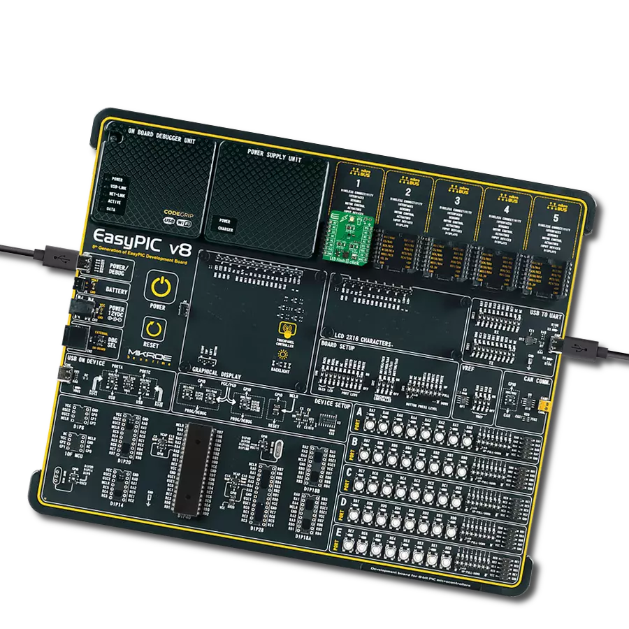
Development board
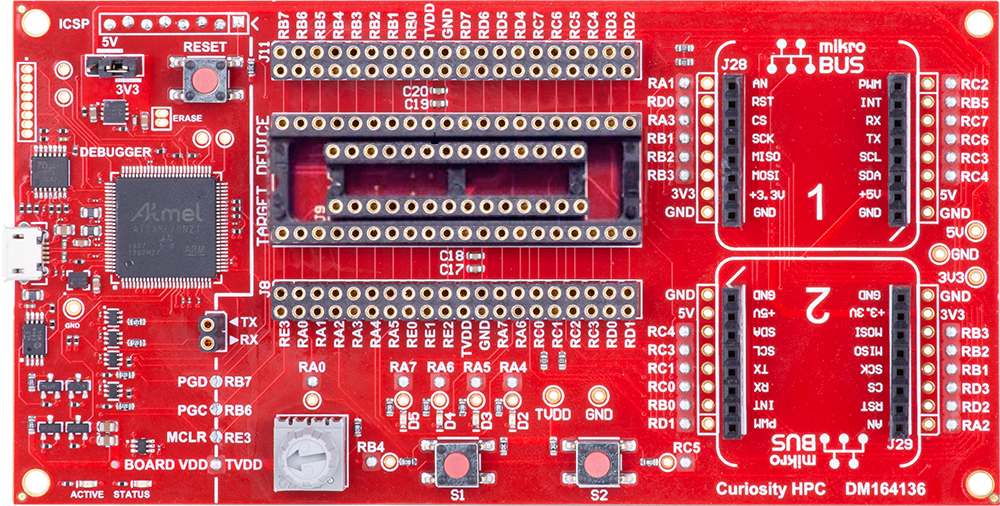
Curiosity HPC, standing for Curiosity High Pin Count (HPC) development board, supports 28- and 40-pin 8-bit PIC MCUs specially designed by Microchip for the needs of rapid development of embedded applications. This board has two unique PDIP sockets, surrounded by dual-row expansion headers, allowing connectivity to all pins on the populated PIC MCUs. It also contains a powerful onboard PICkit™ (PKOB), eliminating the need for an external programming/debugging tool, two mikroBUS™ sockets for Click board™ connectivity, a USB connector, a set of indicator LEDs, push button switches and a variable potentiometer. All
these features allow you to combine the strength of Microchip and Mikroe and create custom electronic solutions more efficiently than ever. Each part of the Curiosity HPC development board contains the components necessary for the most efficient operation of the same board. An integrated onboard PICkit™ (PKOB) allows low-voltage programming and in-circuit debugging for all supported devices. When used with the MPLAB® X Integrated Development Environment (IDE, version 3.0 or higher) or MPLAB® Xpress IDE, in-circuit debugging allows users to run, modify, and troubleshoot their custom software and hardware
quickly without the need for additional debugging tools. Besides, it includes a clean and regulated power supply block for the development board via the USB Micro-B connector, alongside all communication methods that mikroBUS™ itself supports. Curiosity HPC development board allows you to create a new application in just a few steps. Natively supported by Microchip software tools, it covers many aspects of prototyping thanks to many number of different Click boards™ (over a thousand boards), the number of which is growing daily.

Microcontroller Overview
MCU Card / MCU
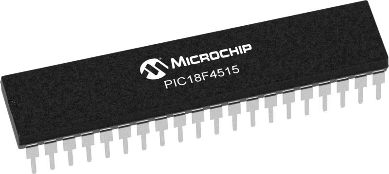
Architecture
PIC
MCU Memory (KB)
48
Silicon Vendor
Microchip
Pin count
40
RAM (Bytes)
3968
Used MCU Pins
mikroBUS™ mapper
Take a closer look
Click board™ Schematic
Step by step
Project assembly
Start by selecting your development board and Click board™. Begin with the Curiosity HPC as your development board.


Track your results in real time
Application Output
1. Application Output - In Debug mode, the 'Application Output' window enables real-time data monitoring, offering direct insight into execution results. Ensure proper data display by configuring the environment correctly using the provided tutorial.

2. UART Terminal - Use the UART Terminal to monitor data transmission via a USB to UART converter, allowing direct communication between the Click board™ and your development system. Configure the baud rate and other serial settings according to your project's requirements to ensure proper functionality. For step-by-step setup instructions, refer to the provided tutorial.

3. Plot Output - The Plot feature offers a powerful way to visualize real-time sensor data, enabling trend analysis, debugging, and comparison of multiple data points. To set it up correctly, follow the provided tutorial, which includes a step-by-step example of using the Plot feature to display Click board™ readings. To use the Plot feature in your code, use the function: plot(*insert_graph_name*, variable_name);. This is a general format, and it is up to the user to replace 'insert_graph_name' with the actual graph name and 'variable_name' with the parameter to be displayed.

Software Support
Library Description
This library contains API for BarGraph 3 Click driver.
Key functions:
bargraph3_display- This function control the displaybargraph3_set_pwm- This function set PWMbargraph3_enable- Functions for enable the chip.
Open Source
Code example
The complete application code and a ready-to-use project are available through the NECTO Studio Package Manager for direct installation in the NECTO Studio. The application code can also be found on the MIKROE GitHub account.
/*!
 * \file
 * \brief BarGraph3 Click example
 *
 * # Description
 * This application used to create various types of VU meters,
 * status indicators, different types of counters and similar devices.
 *
 * The demo application is composed of two sections :
 *
 * ## Application Init
 * Initialization driver init, enable device and set PWM
 *
 * ## Application Task
 * Counter passes through the loop and logs the value of the
 * counter on the bargraph display.
 *
 * \author MikroE Team
 *
 */
// ------------------------------------------------------------------- INCLUDES

#include "board.h"
#include "log.h"
#include "bargraph3.h"

// ------------------------------------------------------------------ VARIABLES

static bargraph3_t bargraph3;
static log_t logger;


void application_init ( void )
{
    log_cfg_t log_cfg;
    bargraph3_cfg_t cfg;

    /**
     * Logger initialization.
     * Default baud rate: 115200
     * Default log level: LOG_LEVEL_DEBUG
     * @note If USB_UART_RX and USB_UART_TX
     * are defined as HAL_PIN_NC, you will
     * need to define them manually for log to work.
     * See @b LOG_MAP_USB_UART macro definition for detailed explanation.
     */
    LOG_MAP_USB_UART( log_cfg );
    log_init( &logger, &log_cfg );
    log_info( &logger, "---- Application Init ----" );

    //  Click initialization.

    bargraph3_cfg_setup( &cfg );
    BARGRAPH3_MAP_MIKROBUS( cfg, MIKROBUS_1 );
    bargraph3_init( &bargraph3, &cfg );

    bargraph3_enable( &bargraph3, BARGRAPH3_DEVICE_ENABLE );
    bargraph3_set_pwm( &bargraph3, BARGRAPH3_DEVICE_ENABLE );
    Delay_ms ( 500 );
}

void application_task ( void )
{
   uint8_t bargraph_cnt;

    for ( bargraph_cnt = 0; bargraph_cnt <= 5; bargraph_cnt++ )
    {
        bargraph3_display( &bargraph3, BARGRAPH3_INCREASE_LED,
                           BARGRAPH3_DIRECTION_BOTTOM_TO_TOP,
                           bargraph_cnt );
        Delay_ms ( 1000 );
    }
}

int main ( void )
{
    /* Do not remove this line or clock might not be set correctly. */
    #ifdef PREINIT_SUPPORTED
    preinit();
    #endif

    application_init( );

    for ( ; ; )
    {
        application_task( );
    }

    return 0;
}


// ------------------------------------------------------------------------ END
Additional Support
Resources
Category:LED Segment