Stay ahead in the world of communication technology with MAX485 and dsPIC33EP512MU810
Transforming data transmission: The magic of RS485 transceivers

Published Oct 19, 2023
Click board™
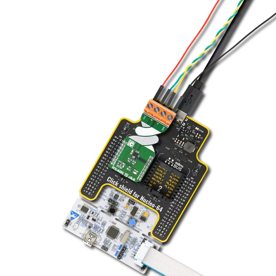
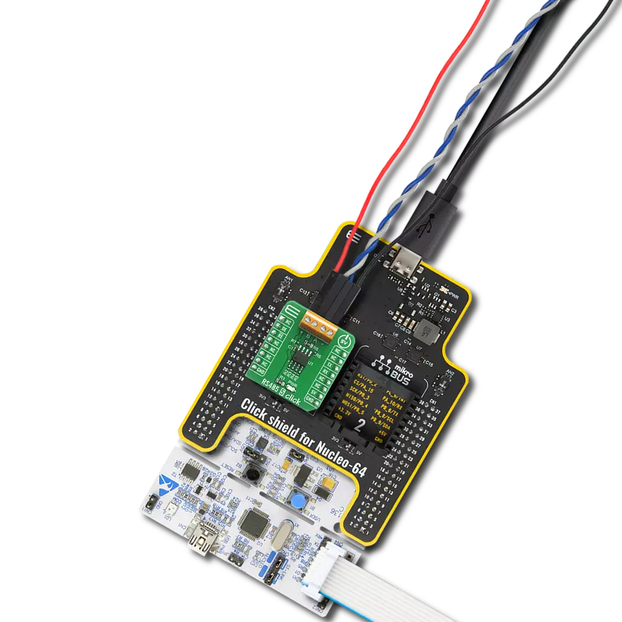
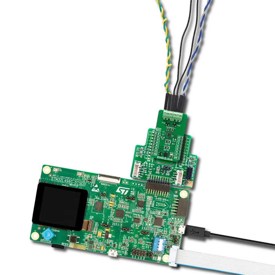
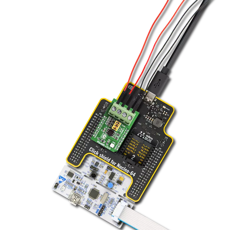
RS485 5 Click
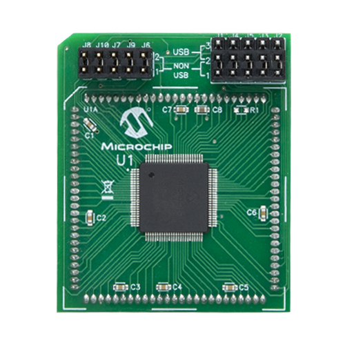
Dev. board
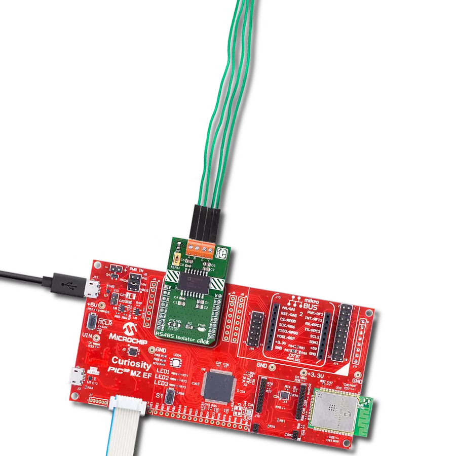
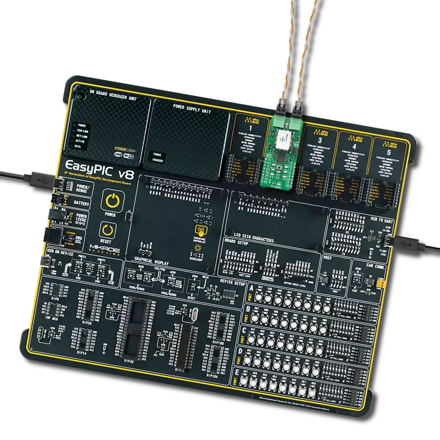
Explorer 16/32 development board
Compiler
NECTO Studio
MCU
dsPIC33EP512MU810
The core purpose of this solution is to establish a robust, long-distance network, facilitating efficient data exchange
A
A
Hardware Overview
How does it work?
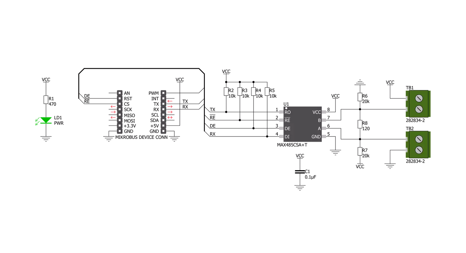
RS485 5 Click is based on the MAX485, low-power, slew-rate-limited transceiver for RS-485 and RS-422 communication from Analog Devices, which draw between 120µA and 500µA of supply current when unloaded or fully loaded with disabled drivers. All parts operate from a single 5V supply. Driver is short-circuit current limited and is protected against excessive power dissipation by thermal shutdown circuitry that places the driver outputs into a high-impedance state. The receiver input has a fail-safe feature that guarantees a logic-high output if the input is open circuit. The MAX485 slew rates are not limited, allowing it to transmit up to 2.5Mbps and half-duplex communication. In general, the maximal transfer
speed is determined by the bus length, longer bus lines will result in less transfer speed. The RS485/422 line should be terminated at both ends in its characteristic impedance and stub lengths off the main line should be kept as short as possible to minimize the reflections. The RS-485/RS-422 standard covers line lengths up to 1220 meters (4000 feet). Excessive output current and power dissipation caused by faults or by bus contention are prevented by two mechanisms. A foldback current limit on the output stage provides immediate protection against short circuits over the whole common-mode voltage range. In addition, a thermal shutdown circuit forces the driver outputs into a high-impedance
state if the temperature rises excessively. There are two 2-pole screw terminals on board (+, B, A, -) for connecting RS422/485 bus twisted pair cable, along with the GND and VCC. The terminal inputs labeled as “A” and “B” are used to connect the bus wires. GND and VCC rails can be used to provide the power supply for another node. Note that the VCC terminal is directly routed to the 5V rail of the mikroBUS™. This Click board™ can be operated only with a 5V logic voltage level. The board must perform appropriate logic voltage level conversion before using MCUs with different logic levels. Also, it comes equipped with a library containing functions and an example code that can be used as a reference for further development.


Features overview
Development board
Explorer 16/32 development board is a flexible and convenient development, demonstration, and testing platform for 16-bit PIC24 MCUs, dsPIC® DSCs, and 32-bit PIC32 MCUs from Microchip Technology. It features all the necessary hardware to develop and debug a complete embedded application. The board accepts Processor Plug-In Modules (PIMs) designed for the Explorer 16 or Explorer 16/32 development board for easy device swapping. In addition to the hardware features provided by the board, hardware expansion is possible through the use of PICtail™ Plus
daughter cards and mikroBUS™ accessory boards. Coupled with the integrated PICkit™-On-Board (PKOB), MPLAB ICD In-Circuit Debugger real-time debug facilities enable faster evaluation and prototyping of applications. This development board supports all the Explorer PIMs. However, not all PIMs are supported by the PKOB. To check the list of supported and unsupported PIMs, refer to the PICkit™ On-Board 3 (PKOB3) Support List. For PIMs not on the PKOB3 support list, use the JP1 or J14 connectors to program the device with a newer generation programming tool. Explorer 16/32
development board offers only the main board, allowing customization of the other necessary components. Choose your PIM based on MCUs and DSCs under consideration from a wide range of Processor Plug-In Modules. This board is optimal for customers migrating from Classic Explorer 16 to the new Explorer 16/32 platform, while all the necessary additional components like Processor Plug-In Modules and PICtail™ Plus Daughter Boards are already available.

Microcontroller Overview
MCU Card / MCU
Architecture
dsPIC
MCU Memory (KB)
512
Silicon Vendor
Microchip
Pin count
100
RAM (Bytes)
53248
Used MCU Pins
mikroBUS™ mapper
Take a closer look
Click board™ Schematic
Step by step
Project assembly

Start by selecting your development board and Click board™. Begin with the Explorer 16/32 development board as your development board.


Track your results in real time
Application Output
1. Application Output - In Debug mode, the 'Application Output' window enables real-time data monitoring, offering direct insight into execution results. Ensure proper data display by configuring the environment correctly using the provided tutorial.

2. UART Terminal - Use the UART Terminal to monitor data transmission via a USB to UART converter, allowing direct communication between the Click board™ and your development system. Configure the baud rate and other serial settings according to your project's requirements to ensure proper functionality. For step-by-step setup instructions, refer to the provided tutorial.

3. Plot Output - The Plot feature offers a powerful way to visualize real-time sensor data, enabling trend analysis, debugging, and comparison of multiple data points. To set it up correctly, follow the provided tutorial, which includes a step-by-step example of using the Plot feature to display Click board™ readings. To use the Plot feature in your code, use the function: plot(*insert_graph_name*, variable_name);. This is a general format, and it is up to the user to replace 'insert_graph_name' with the actual graph name and 'variable_name' with the parameter to be displayed.

Software Support
Library Description
This library contains API for RS485 5 Click driver.
Key functions:
rs4855_generic_write- Generic write function.rs4855_set_de_state- Sets DE pin to high or low state.rs4855_set_re_state- Sets RE pin to high or low state.
Open Source
Code example
The complete application code and a ready-to-use project are available through the NECTO Studio Package Manager for direct installation in the NECTO Studio. The application code can also be found on the MIKROE GitHub account.
/*!
 * \file
 * \brief Rs4855 Click example
 *
 * # Description
 * This example reads and processes data from RS485 5 Clicks.
 *
 * The demo application is composed of two sections :
 *
 * ## Application Init
 * Initializes the driver and enables the selected mode.
 *
 * ## Application Task
 * Depending on the selected mode, it reads all the received data or sends the desired message
 * every 2 seconds.
 *
 * ## Additional Function
 * - rs4855_process ( ) - The general process of collecting the received data.
 *
 * \author MikroE Team
 *
 */
// ------------------------------------------------------------------- INCLUDES

#include "board.h"
#include "log.h"
#include "rs4855.h"
#include "string.h"

#define PROCESS_RX_BUFFER_SIZE 500

#define TEXT_TO_SEND "MikroE\r\n"

// ------------------------------------------------------------------ VARIABLES

#define DEMO_APP_RECEIVER
// #define DEMO_APP_TRANSMITTER

static rs4855_t rs4855;
static log_t logger;

// ------------------------------------------------------- ADDITIONAL FUNCTIONS

static void rs4855_process ( void )
{
    int32_t rsp_size;

    char uart_rx_buffer[ PROCESS_RX_BUFFER_SIZE ] = { 0 };
    uint8_t check_buf_cnt;

    rsp_size = rs4855_generic_read( &rs4855, uart_rx_buffer, PROCESS_RX_BUFFER_SIZE );

    if ( rsp_size >= strlen( TEXT_TO_SEND ) )
    {
        log_printf( &logger, "Received data: " );

        for ( check_buf_cnt = 0; check_buf_cnt < rsp_size; check_buf_cnt++ )
        {
            log_printf( &logger, "%c", uart_rx_buffer[ check_buf_cnt ] );
        }
    }
    Delay_ms ( 100 );
}

// ------------------------------------------------------ APPLICATION FUNCTIONS

void application_init ( void )
{
    log_cfg_t log_cfg;
    rs4855_cfg_t cfg;

    /**
     * Logger initialization.
     * Default baud rate: 115200
     * Default log level: LOG_LEVEL_DEBUG
     * @note If USB_UART_RX and USB_UART_TX
     * are defined as HAL_PIN_NC, you will
     * need to define them manually for log to work.
     * See @b LOG_MAP_USB_UART macro definition for detailed explanation.
     */
    LOG_MAP_USB_UART( log_cfg );
    log_init( &logger, &log_cfg );
    log_info( &logger, "---- Application Init ----" );

    //  Click initialization.

    rs4855_cfg_setup( &cfg );
    RS4855_MAP_MIKROBUS( cfg, MIKROBUS_1 );
    rs4855_init( &rs4855, &cfg );

    Delay_ms ( 100 );

#ifdef DEMO_APP_RECEIVER
    rs4855_set_re_state( &rs4855, RS4855_PIN_STATE_LOW );
    rs4855_set_de_state( &rs4855, RS4855_PIN_STATE_LOW );
    log_info( &logger, "---- Receiver mode ----" );
#endif
#ifdef DEMO_APP_TRANSMITTER
    rs4855_set_re_state( &rs4855, RS4855_PIN_STATE_HIGH );
    rs4855_set_de_state( &rs4855, RS4855_PIN_STATE_HIGH );
    log_info( &logger, "---- Transmitter mode ----" );
#endif
}

void application_task ( void )
{
#ifdef DEMO_APP_RECEIVER
    rs4855_process( );
#endif

#ifdef DEMO_APP_TRANSMITTER
    rs4855_generic_write( &rs4855, TEXT_TO_SEND, 8 );
    log_info( &logger, "---- Data sent ----" );
    Delay_ms ( 1000 );
    Delay_ms ( 1000 );
#endif
}

int main ( void )
{
    /* Do not remove this line or clock might not be set correctly. */
    #ifdef PREINIT_SUPPORTED
    preinit();
    #endif

    application_init( );

    for ( ; ; )
    {
        application_task( );
    }

    return 0;
}


// ------------------------------------------------------------------------ END