Say goodbye to data loss worries with CY14B101I and PIC18F57Q43
nvSRAM: Where data lives forever
Published Feb 13, 2024
Click board™
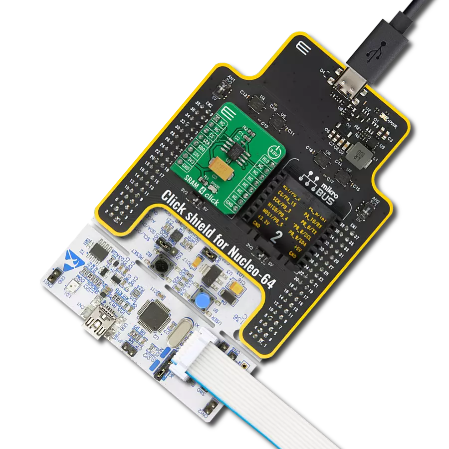
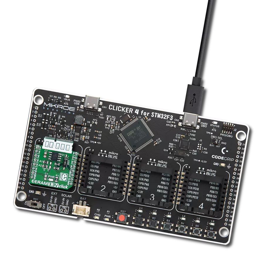
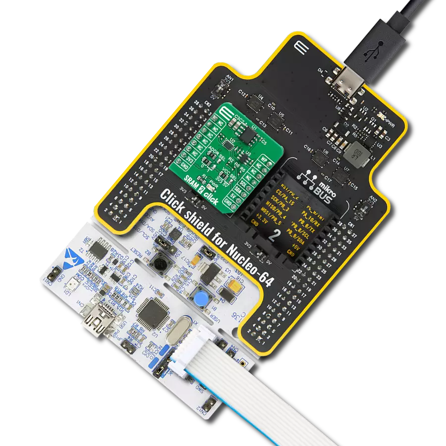
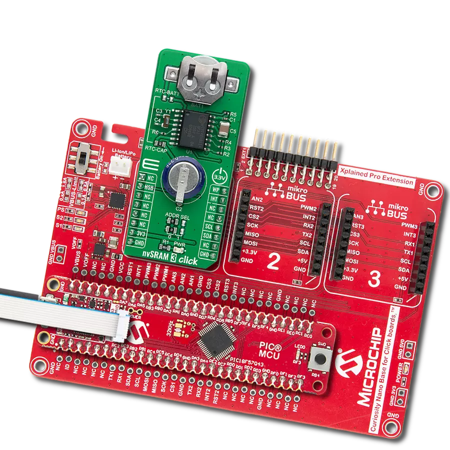
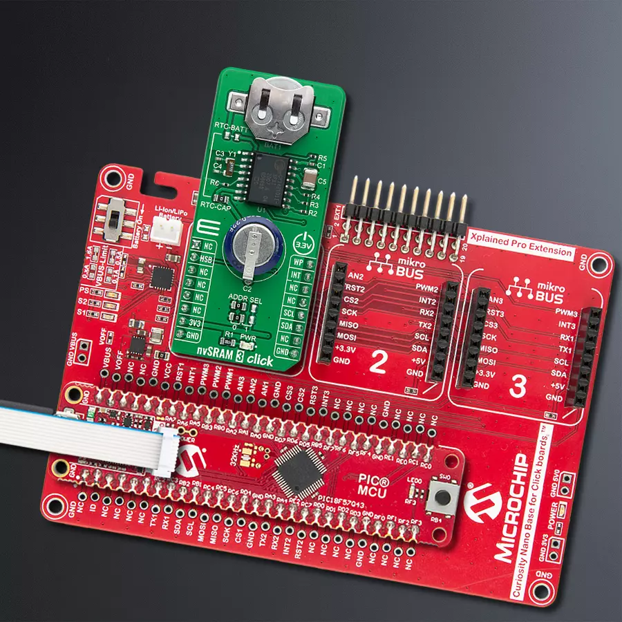
nvSRAM 3 Click
Dev. board
Curiosity Nano with PIC18F57Q43
Compiler
NECTO Studio
MCU
PIC18F57Q43
Trust nvSRAM as your data's timeless vault, ensuring that precious memories stay alive and intact
A
A
Hardware Overview
How does it work?
nvSRAM 3 Click as its foundation uses the CY14B101I, a 1-Mbit nvSRAM organized as 128K words of 8 bits each with a fully-featured real-time clock from Infineon. The CY14B101I specifies one million endurance cycles for cells with data retention of a minimum of 20 years, while the QuantumTrap cells provide highly reliable, nonvolatile data storage. In system power loss, data from the SRAM is automatically transferred to its nonvolatile cell using energy stored in a capacitor labeled as C2. During the Power-Up, data from the nonvolatile cell is recalled automatically in the SRAM array and available to the user. The endurance cycle consumes when data transfer happens from the SRAM cells to nonvolatile cells during the Power-Down. This Click board™ can be permanently powered by placing jumpers labeled as RTC-CAP or RTC-BATT. The CY14B101I uses an external battery power source from the button cell battery holder by utilizing an automatic backup. It is suitable for
12mm Coin Cell batteries when there is no power supply on its main power terminals, allowing for uninterrupted operation. nvSRAM 3 Click communicates with MCU using a standard I2C 2-Wire interface, with clock frequencies up to 100kHz in the Standard, 400kHz in the Fast, 1MHz in FastPlus, and up to 3.4MHz in High-Speed Mode. The CY14B101I offers zero cycle delay write operation with infinite SRAM write endurance. It also allows the choice of the least significant bit (LSB) of its I2C slave address by positioning SMD jumpers labeled ADDR SEL to an appropriate position marked as 0 and 1. An additional feature of this Click board™ represents the Write Protection and Interrupt functions labeled as WP and INT routed on the PWM and INT pins of the mikroBUS™ socket. The WP pin is an active-high pin that protects the entire memory and all registers from write operations. MCU must hold the WP pin high to inhibit all the write operations. When this pin is high, all memory and register
writes are prohibited, and the address counter does not increment. On the other hand, the CY14B101I can use an INT pin in several ways, such as interrupt output, calibration, or a square wave, programmable to respond to the clock alarm, the watchdog timer, and the power monitor. The STORE operation of the CY14B101I can be controlled and acknowledged via the HSB pin, routed on the RST pin of the mikroBUS™ socket. If no STORE/RECALL is in progress, the CY14B101I can use this pin to request a hardware STORE cycle. When the HSB pin is in a LOW logic state, the CY14B101I conditionally initiates a STORE operation. This Click board™ can be operated only with a 3.3V logic voltage level. The board must perform appropriate logic voltage level conversion before using MCUs with different logic levels. Also, it comes equipped with a library containing functions and an example code that can be used for further development.

Features overview
Development board
PIC18F57Q43 Curiosity Nano evaluation kit is a cutting-edge hardware platform designed to evaluate microcontrollers within the PIC18-Q43 family. Central to its design is the inclusion of the powerful PIC18F57Q43 microcontroller (MCU), offering advanced functionalities and robust performance. Key features of this evaluation kit include a yellow user LED and a responsive
mechanical user switch, providing seamless interaction and testing. The provision for a 32.768kHz crystal footprint ensures precision timing capabilities. With an onboard debugger boasting a green power and status LED, programming and debugging become intuitive and efficient. Further enhancing its utility is the Virtual serial port (CDC) and a debug GPIO channel (DGI
GPIO), offering extensive connectivity options. Powered via USB, this kit boasts an adjustable target voltage feature facilitated by the MIC5353 LDO regulator, ensuring stable operation with an output voltage ranging from 1.8V to 5.1V, with a maximum output current of 500mA, subject to ambient temperature and voltage constraints.

Microcontroller Overview
MCU Card / MCU

Architecture
PIC
MCU Memory (KB)
128
Silicon Vendor
Microchip
Pin count
48
RAM (Bytes)
8196
You complete me!
Accessories
Curiosity Nano Base for Click boards is a versatile hardware extension platform created to streamline the integration between Curiosity Nano kits and extension boards, tailored explicitly for the mikroBUS™-standardized Click boards and Xplained Pro extension boards. This innovative base board (shield) offers seamless connectivity and expansion possibilities, simplifying experimentation and development. Key features include USB power compatibility from the Curiosity Nano kit, alongside an alternative external power input option for enhanced flexibility. The onboard Li-Ion/LiPo charger and management circuit ensure smooth operation for battery-powered applications, simplifying usage and management. Moreover, the base incorporates a fixed 3.3V PSU dedicated to target and mikroBUS™ power rails, alongside a fixed 5.0V boost converter catering to 5V power rails of mikroBUS™ sockets, providing stable power delivery for various connected devices.

Used MCU Pins
mikroBUS™ mapper
Take a closer look
Click board™ Schematic

Step by step
Project assembly

Start by selecting your development board and Click board™. Begin with the Curiosity Nano with PIC18F57Q43 as your development board.


Track your results in real time
Application Output
1. Application Output - In Debug mode, the 'Application Output' window enables real-time data monitoring, offering direct insight into execution results. Ensure proper data display by configuring the environment correctly using the provided tutorial.

2. UART Terminal - Use the UART Terminal to monitor data transmission via a USB to UART converter, allowing direct communication between the Click board™ and your development system. Configure the baud rate and other serial settings according to your project's requirements to ensure proper functionality. For step-by-step setup instructions, refer to the provided tutorial.

3. Plot Output - The Plot feature offers a powerful way to visualize real-time sensor data, enabling trend analysis, debugging, and comparison of multiple data points. To set it up correctly, follow the provided tutorial, which includes a step-by-step example of using the Plot feature to display Click board™ readings. To use the Plot feature in your code, use the function: plot(*insert_graph_name*, variable_name);. This is a general format, and it is up to the user to replace 'insert_graph_name' with the actual graph name and 'variable_name' with the parameter to be displayed.

Software Support
Library Description
This library contains API for nvSRAM 3 Click driver.
Key functions:
nvsram3_memory_write- This function write a desired number of data bytes starting from the selected memory address by using I2C serial interface.nvsram3_memory_read- This function reads a desired number of data bytes starting from the selected memory address by using I2C serial interface.nvsram3_get_rtc_time- This function get RTC time data structure.
Open Source
Code example
The complete application code and a ready-to-use project are available through the NECTO Studio Package Manager for direct installation in the NECTO Studio. The application code can also be found on the MIKROE GitHub account.
/*!
 * @file main.c
 * @brief nvSRAM3 Click example
 *
 * # Description
 * The demo application shows how to write/read data to/from nvSRAM memory.
 * It also sets RTC date and time, then reads it in an infinite loop and displays results on USB UART each second.
 *
 * The demo application is composed of two sections :
 *
 * ## Application Init
 * Initializes device, reads the device ID, writes desired message to memory and sets RTC date and time.
 *
 * ## Application Task
 * Reads current date and time and then reads the message that we have previusly stored in the memory.
 * All data is being logged on USB UART.
 *
 * @author Stefan Filipovic
 *
 */

#include "board.h"
#include "log.h"
#include "nvsram3.h"

static nvsram3_t nvsram3;
static log_t logger;

static char demo_data[ 9 ] = { 'M', 'i', 'k', 'r', 'o', 'E', 13 ,10 , 0 };
static char rx_data[ 9 ];
static uint32_t memory_addr;
static uint8_t new_sec = 255;
static uint16_t c_year = 2020;

static nvsram3_rtc_time_t time;
static nvsram3_rtc_date_t date;

void application_init ( void )
{
    log_cfg_t log_cfg;  /**< Logger config object. */
    nvsram3_cfg_t nvsram3_cfg;  /**< Click config object. */

    /**
     * Logger initialization.
     * Default baud rate: 115200
     * Default log level: LOG_LEVEL_DEBUG
     * @note If USB_UART_RX and USB_UART_TX
     * are defined as HAL_PIN_NC, you will
     * need to define them manually for log to work.
     * See @b LOG_MAP_USB_UART macro definition for detailed explanation.
     */
    LOG_MAP_USB_UART( log_cfg );
    log_init( &logger, &log_cfg );
    log_info( &logger, " Application Init " );

    // Click initialization.

    nvsram3_cfg_setup( &nvsram3_cfg );
    NVSRAM3_MAP_MIKROBUS( nvsram3_cfg, MIKROBUS_1 );
    err_t init_flag = nvsram3_init( &nvsram3, &nvsram3_cfg );

    if ( init_flag == I2C_MASTER_ERROR )
    {
        log_error( &logger, " Application Init Error. " );
        log_info( &logger, " Please, run program again... " );

        for ( ; ; );
    }

    log_printf( &logger, "-----------------------\r\n" );
    log_printf( &logger, "     nvSRAM 3 Click    \r\n" );
    log_printf( &logger, "-----------------------\r\n" );

    nvsram3_default_cfg ( &nvsram3 );
    Delay_ms ( 100 );

    log_printf( &logger, " DEVICE ID: 0x%.8LX\r\n", nvsram3_get_device_id( &nvsram3 ) );
    log_printf( &logger, "-----------------------\r\n" );
    Delay_ms ( 100 );

    memory_addr = 0x10000;

    log_printf( &logger, "  Write data : %s", demo_data );
    nvsram3_memory_write( &nvsram3, memory_addr, &demo_data[ 0 ], 9 );
    log_printf( &logger, "-----------------------\r\n" );
    Delay_ms ( 1000 );

    date.day_of_week = 4;
    date.day = 31;
    date.month = 12;
    date.year = 2020;
    nvsram3_set_rtc_date( &nvsram3, date );
    Delay_ms ( 100 );

    time.hours = 23;
    time.min = 59;
    time.sec = 50;
    nvsram3_set_rtc_time( &nvsram3, time );
    Delay_ms ( 100 );
}

void application_task ( void )
{
    nvsram3_get_rtc_time( &nvsram3, &time );
    nvsram3_get_rtc_date( &nvsram3, &date );

    if ( time.sec != new_sec )
    {
        log_printf( &logger, "  Date      : %.2d-%.2d-%.4d\r\n", ( uint16_t ) date.day, ( uint16_t ) date.month, ( uint16_t ) date.year );
        log_printf( &logger, "  Time      : %.2d:%.2d:%.2d\r\n", ( uint16_t ) time.hours, ( uint16_t ) time.min, ( uint16_t ) time.sec );
        log_printf( &logger, "- - - - - - - - - - - - - - -\r\n" );
        new_sec = time.sec;

        if ( date.year != c_year )
        {
            log_printf( &logger, "     Happy New Year    \r\n" );
            c_year = date.year;
        }
        else
        {
            nvsram3_memory_read( &nvsram3, memory_addr, &rx_data[ 0 ], 9 );
            log_printf( &logger, "  Read data : %s", rx_data );
        }

        log_printf( &logger, "-----------------------\r\n" );
    }
    else
    {
        Delay_ms ( 500 );
    }
}

int main ( void )
{
    /* Do not remove this line or clock might not be set correctly. */
    #ifdef PREINIT_SUPPORTED
    preinit();
    #endif

    application_init( );

    for ( ; ; )
    {
        application_task( );
    }

    return 0;
}

// ------------------------------------------------------------------------ END
Additional Support
Resources
Category:SRAM