Add DRAM memory to your design with APS6404L-3SQR and ATmega328
Put your memory to good use!

Published Feb 14, 2024
Click board™
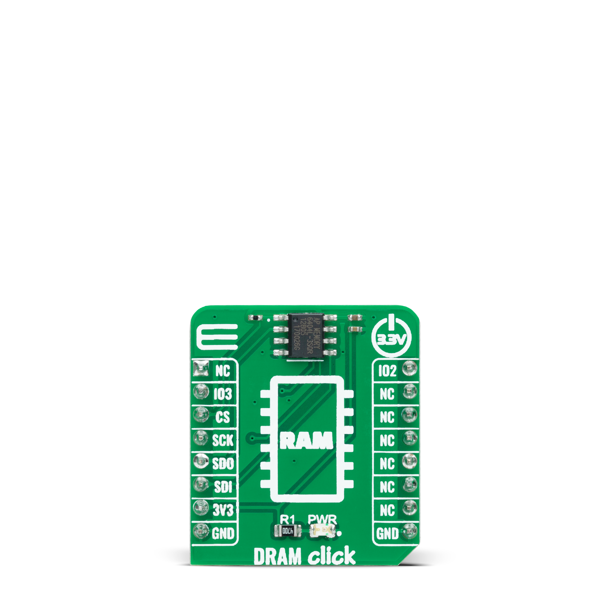
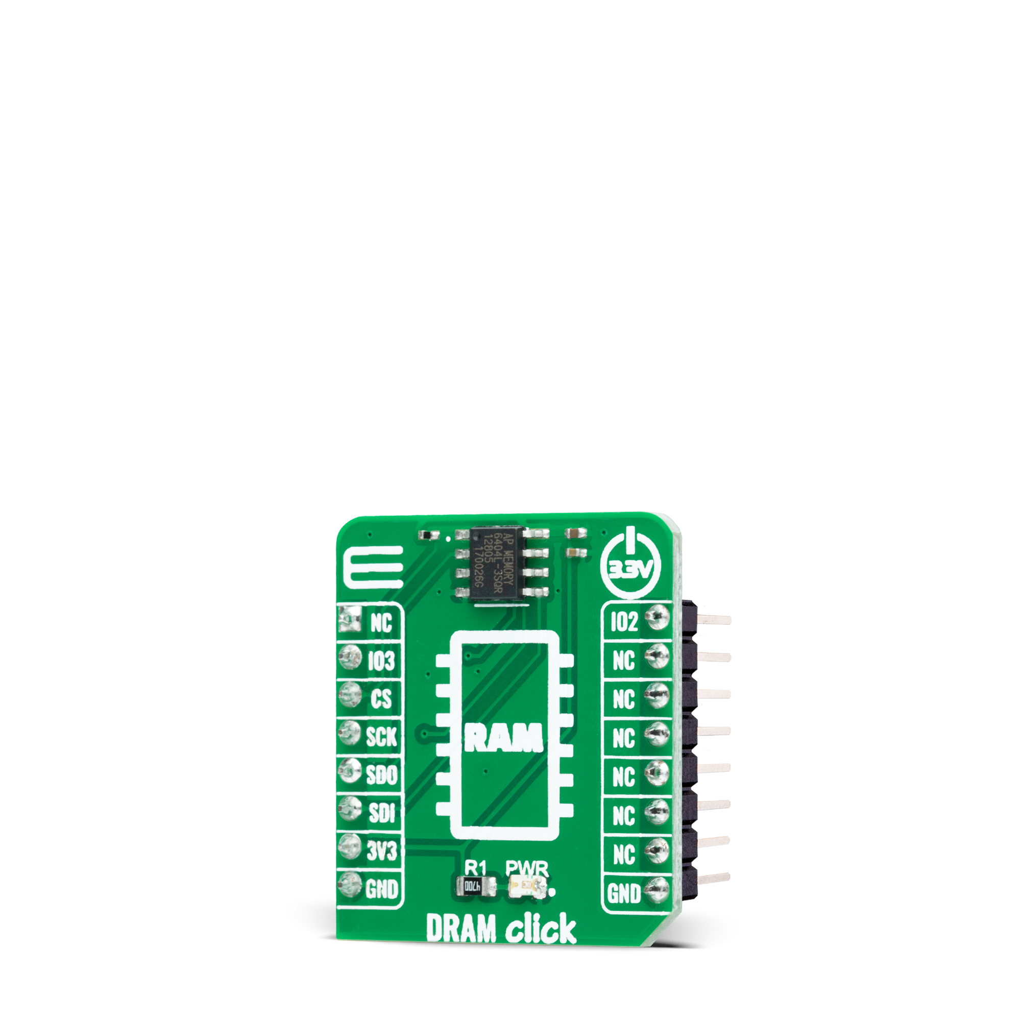
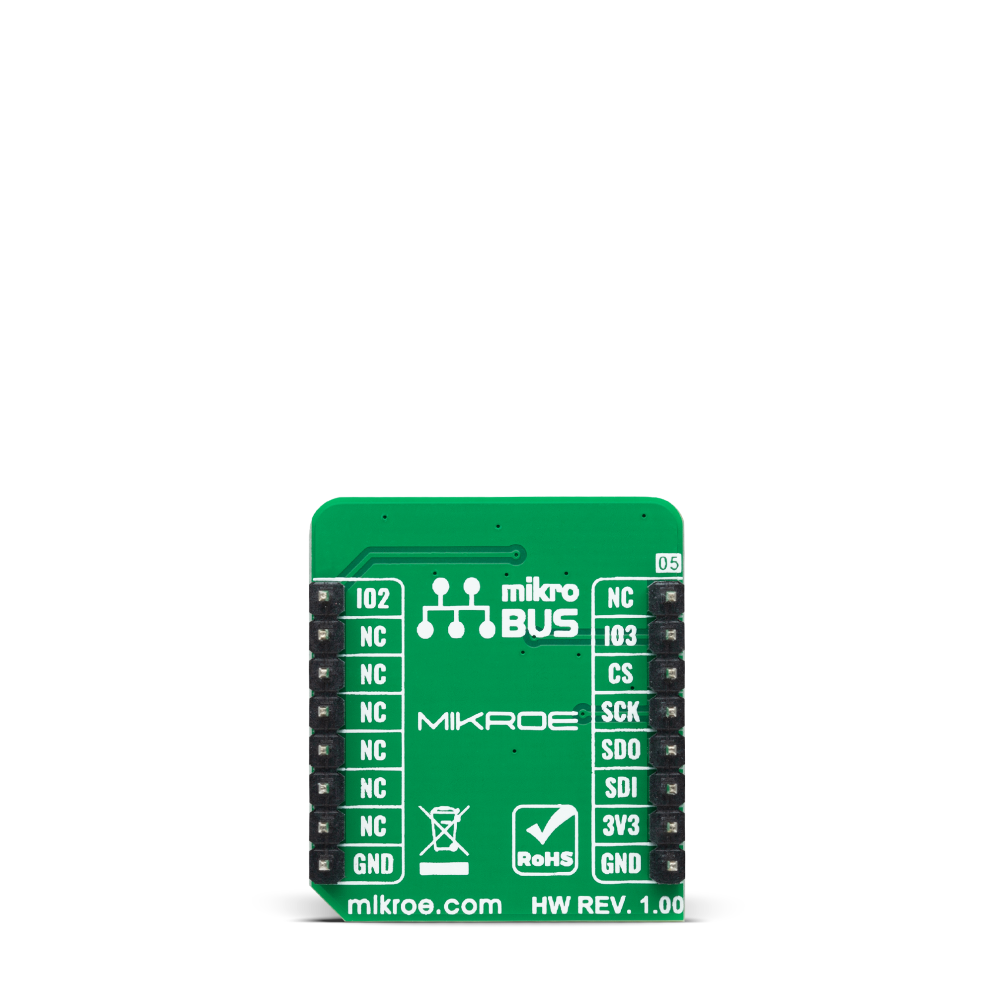
DRAM Click
Dev. board
Arduino UNO Rev3
Compiler
NECTO Studio
MCU
ATmega328
Secure your information with a quality DRAM memory
A
A
Hardware Overview
How does it work?
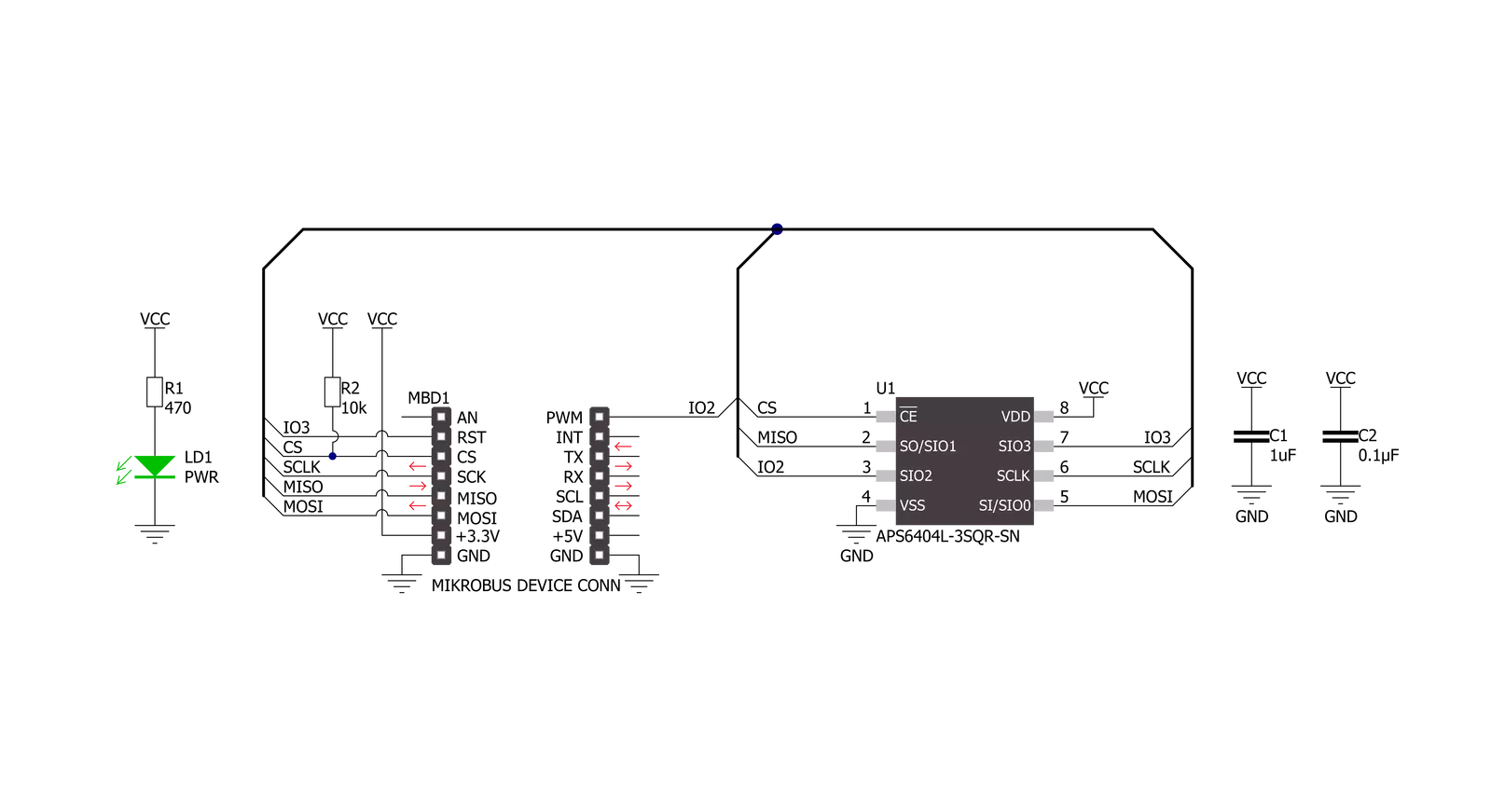
DRAM Click is based on the APS6404L-3SQR, a 64Mb PSRAM (Pseudo-SRAM) memory with an SPI/QPI interface from AP Memory. Organized as 8M x 8 bits each, this high-speed, high-performance memory has a page size of 1024 bytes. It also incorporates a seamless, self-managed refresh mechanism specially designed to maximize the performance of the memory read operation (it does not require the support of DRAM refresh from the system host). It is most suitable for low-power and low-cost portable applications.
The APS6404L-3SQR communicates with the MCU using an SPI serial interface that also supports Quad SPI and the two most common modes, SPI Mode 0 (QSPI Mode 1), with a maximum SPI frequency of 133MHz. The APS6404L-3SQR includes an on-chip voltage sensor used to start the self-initialization process. When the main power supply voltage reaches a stable level at or above the minimum supply voltage level, the device will require 150μs and user-issued RESET Operation to complete its self-initialization
process. The device powers up in SPI mode by default but can also switch to QPI mode. The CS pin must be set to high logic level before initiating any operations. This Click board™ can only be operated with a 3.3V logic voltage level. The board must perform appropriate logic voltage level conversion before using MCUs with different logic levels. However, the Click board™ comes equipped with a library containing functions and an example code that can be used as a reference for further development.
Features overview
Development board
Arduino UNO is a versatile microcontroller board built around the ATmega328P chip. It offers extensive connectivity options for various projects, featuring 14 digital input/output pins, six of which are PWM-capable, along with six analog inputs. Its core components include a 16MHz ceramic resonator, a USB connection, a power jack, an
ICSP header, and a reset button, providing everything necessary to power and program the board. The Uno is ready to go, whether connected to a computer via USB or powered by an AC-to-DC adapter or battery. As the first USB Arduino board, it serves as the benchmark for the Arduino platform, with "Uno" symbolizing its status as the
first in a series. This name choice, meaning "one" in Italian, commemorates the launch of Arduino Software (IDE) 1.0. Initially introduced alongside version 1.0 of the Arduino Software (IDE), the Uno has since become the foundational model for subsequent Arduino releases, embodying the platform's evolution.

Microcontroller Overview
MCU Card / MCU
Architecture
AVR
MCU Memory (KB)
32
Silicon Vendor
Microchip
Pin count
32
RAM (Bytes)
2048
You complete me!
Accessories
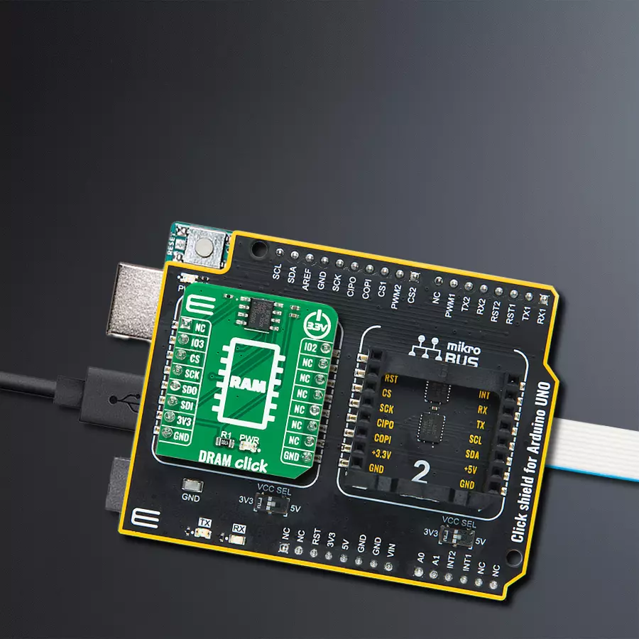
Click Shield for Arduino UNO has two proprietary mikroBUS™ sockets, allowing all the Click board™ devices to be interfaced with the Arduino UNO board without effort. The Arduino Uno, a microcontroller board based on the ATmega328P, provides an affordable and flexible way for users to try out new concepts and build prototypes with the ATmega328P microcontroller from various combinations of performance, power consumption, and features. The Arduino Uno has 14 digital input/output pins (of which six can be used as PWM outputs), six analog inputs, a 16 MHz ceramic resonator (CSTCE16M0V53-R0), a USB connection, a power jack, an ICSP header, and reset button. Most of the ATmega328P microcontroller pins are brought to the IO pins on the left and right edge of the board, which are then connected to two existing mikroBUS™ sockets. This Click Shield also has several switches that perform functions such as selecting the logic levels of analog signals on mikroBUS™ sockets and selecting logic voltage levels of the mikroBUS™ sockets themselves. Besides, the user is offered the possibility of using any Click board™ with the help of existing bidirectional level-shifting voltage translators, regardless of whether the Click board™ operates at a 3.3V or 5V logic voltage level. Once you connect the Arduino UNO board with our Click Shield for Arduino UNO, you can access hundreds of Click boards™, working with 3.3V or 5V logic voltage levels.

Used MCU Pins
mikroBUS™ mapper
Take a closer look
Click board™ Schematic
Step by step
Project assembly

Start by selecting your development board and Click board™. Begin with the Arduino UNO Rev3 as your development board.


Software Support
Library Description
This library contains API for DRAM Click driver.
Key functions:
dram_memory_writeThis function writes a desired number of data bytes starting from the selected memory address.dram_memory_readThis function reads a desired number of data bytes starting from the selected memory address.dram_memory_read_fastThis function reads a desired number of data bytes starting from the selected memory address performing a fast read feature.
Open Source
Code example
The complete application code and a ready-to-use project are available through the NECTO Studio Package Manager for direct installation in the NECTO Studio. The application code can also be found on the MIKROE GitHub account.
/*!
 * @file main.c
 * @brief DRAM Click example
 *
 * # Description
 * This example demonstrates the use of DRAM Click board by writing specified data to
 * the memory and reading it back.
 *
 * The demo application is composed of two sections :
 *
 * ## Application Init
 * Initializes the driver, resets the device and checks the communication by reading
 * and verifying the device ID.
 *
 * ## Application Task
 * Writes a desired number of bytes to the memory and then verifies if it is written correctly
 * by reading from the same memory location and displaying the memory content on the USB UART.
 *
 * @author Stefan Filipovic
 *
 */

#include "board.h"
#include "log.h"
#include "dram.h"

#define DEMO_TEXT_MESSAGE_1     "MikroE"
#define DEMO_TEXT_MESSAGE_2     "DRAM Click"
#define STARTING_ADDRESS        0x012345ul

static dram_t dram;
static log_t logger;

void application_init ( void )
{
    log_cfg_t log_cfg;  /**< Logger config object. */
    dram_cfg_t dram_cfg;  /**< Click config object. */

    /**
     * Logger initialization.
     * Default baud rate: 115200
     * Default log level: LOG_LEVEL_DEBUG
     * @note If USB_UART_RX and USB_UART_TX
     * are defined as HAL_PIN_NC, you will
     * need to define them manually for log to work.
     * See @b LOG_MAP_USB_UART macro definition for detailed explanation.
     */
    LOG_MAP_USB_UART( log_cfg );
    log_init( &logger, &log_cfg );
    log_info( &logger, " Application Init " );

    // Click initialization.
    dram_cfg_setup( &dram_cfg );
    DRAM_MAP_MIKROBUS( dram_cfg, MIKROBUS_1 );
    if ( SPI_MASTER_ERROR == dram_init( &dram, &dram_cfg ) )
    {
        log_error( &logger, " Communication init." );
        for ( ; ; );
    }

    if ( DRAM_ERROR == dram_reset ( &dram ) )
    {
        log_error( &logger, " Reset device." );
        for ( ; ; );
    }
    Delay_ms ( 100 );

    if ( DRAM_ERROR == dram_check_communication ( &dram ) )
    {
        log_error( &logger, " Check communication." );
        for ( ; ; );
    }

    log_info( &logger, " Application Task " );
}

void application_task ( void )
{
    uint8_t data_buf[ 128 ] = { 0 };
    log_printf ( &logger, " Memory address: 0x%.6LX\r\n", ( uint32_t ) STARTING_ADDRESS );
    memcpy ( data_buf, DEMO_TEXT_MESSAGE_1, strlen ( DEMO_TEXT_MESSAGE_1 ) );
    if ( DRAM_OK == dram_memory_write ( &dram, STARTING_ADDRESS, data_buf, sizeof ( data_buf ) ) )
    {
        log_printf ( &logger, " Write data: %s\r\n", data_buf );
        Delay_ms ( 100 );
    }
    memset ( data_buf, 0, sizeof ( data_buf ) );
    if ( DRAM_OK == dram_memory_read ( &dram, STARTING_ADDRESS,
                                             data_buf, sizeof ( data_buf ) ) )
    {
        log_printf ( &logger, " Read data: %s\r\n\n", data_buf );
        Delay_ms ( 1000 );
        Delay_ms ( 1000 );
        Delay_ms ( 1000 );
    }
    log_printf ( &logger, " Memory address: 0x%.6LX\r\n", ( uint32_t ) STARTING_ADDRESS );
    memcpy ( data_buf, DEMO_TEXT_MESSAGE_2, strlen ( DEMO_TEXT_MESSAGE_2 ) );
    if ( DRAM_OK == dram_memory_write ( &dram, STARTING_ADDRESS, data_buf, sizeof ( data_buf ) ) )
    {
        log_printf ( &logger, " Write data: %s\r\n", data_buf );
        Delay_ms ( 100 );
    }
    memset ( data_buf, 0, sizeof ( data_buf ) );
    if ( DRAM_OK == dram_memory_read_fast ( &dram, STARTING_ADDRESS, data_buf, sizeof ( data_buf ) ) )
    {
        log_printf ( &logger, " Fast read data : %s\r\n\n", data_buf );
        Delay_ms ( 1000 );
        Delay_ms ( 1000 );
        Delay_ms ( 1000 );
    }
}

int main ( void )
{
    /* Do not remove this line or clock might not be set correctly. */
    #ifdef PREINIT_SUPPORTED
    preinit();
    #endif

    application_init( );

    for ( ; ; )
    {
        application_task( );
    }

    return 0;
}

// ------------------------------------------------------------------------ END
Additional Support
Resources
Category:DRAM