Unlock the potential of data storage with MB85AS4MT and ATmega328P
ReRAM: Your gateway to speed, efficiency, and data density

Published Feb 14, 2024
Click board™
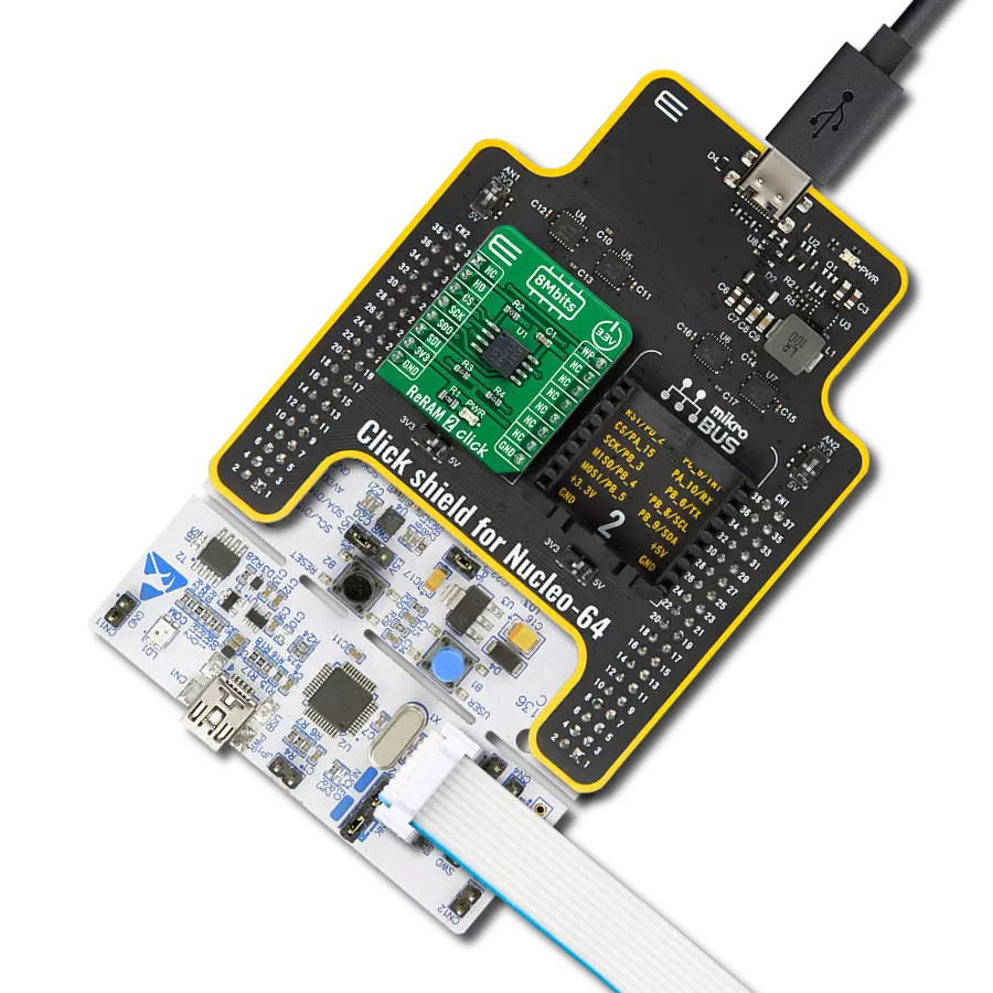
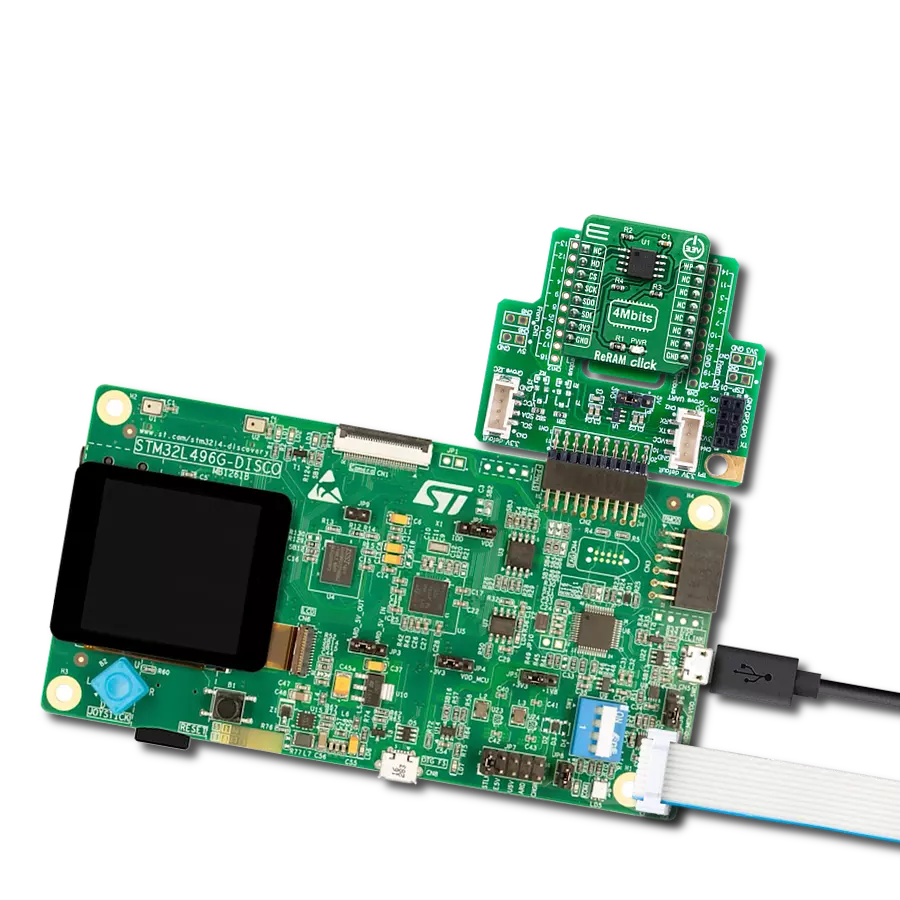
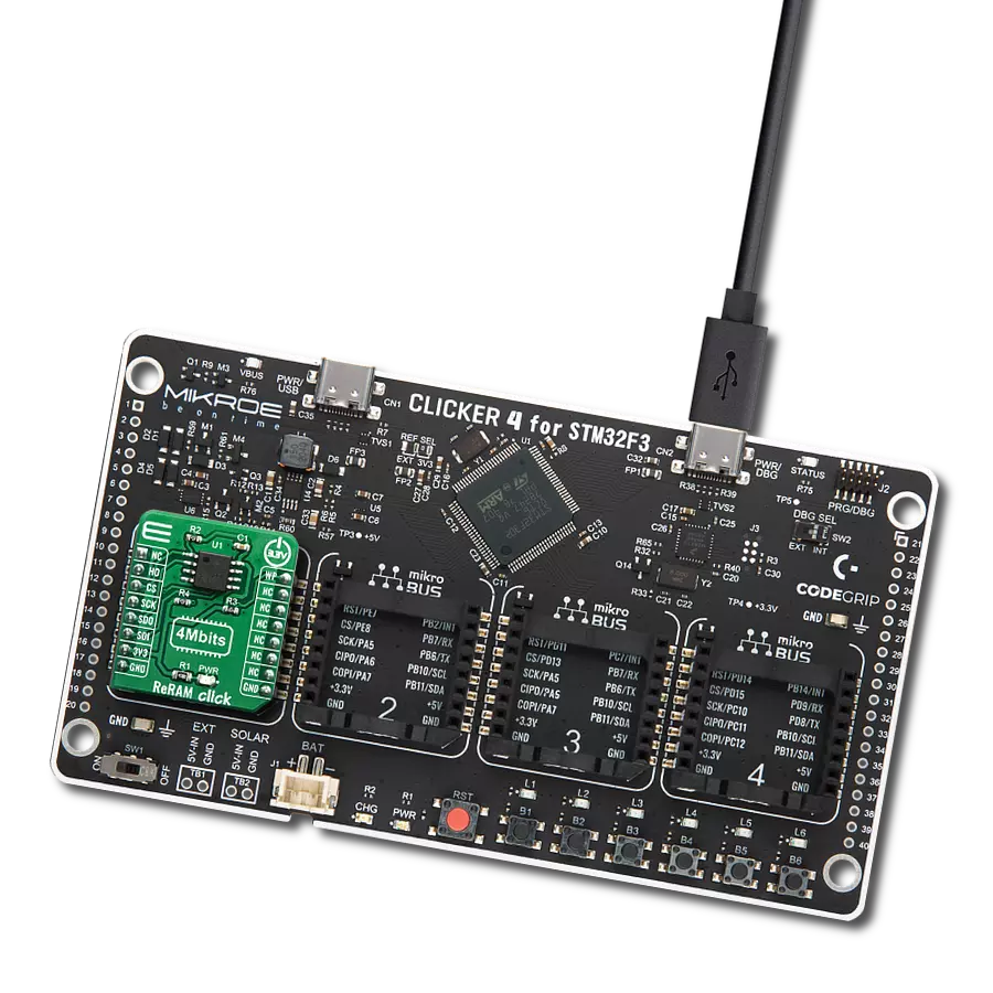
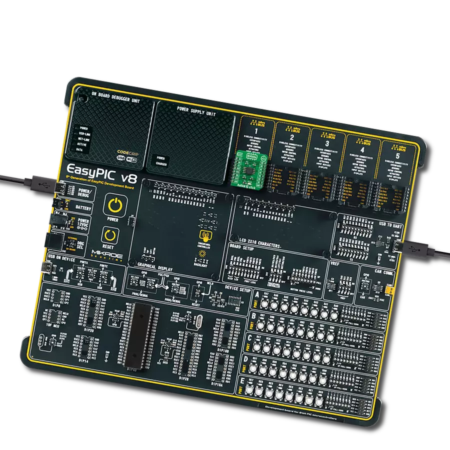
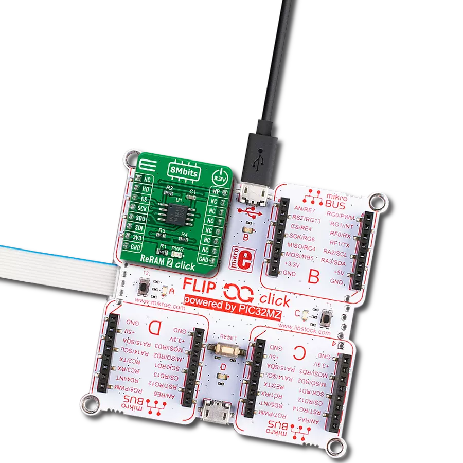
ReRAM Click
Dev. board
Arduino UNO Rev3
Compiler
NECTO Studio
MCU
ATmega328P
Explore how ReRAM is reshaping the memory landscape, delivering faster, more efficient data storage solutions for the modern world
A
A
Hardware Overview
How does it work?
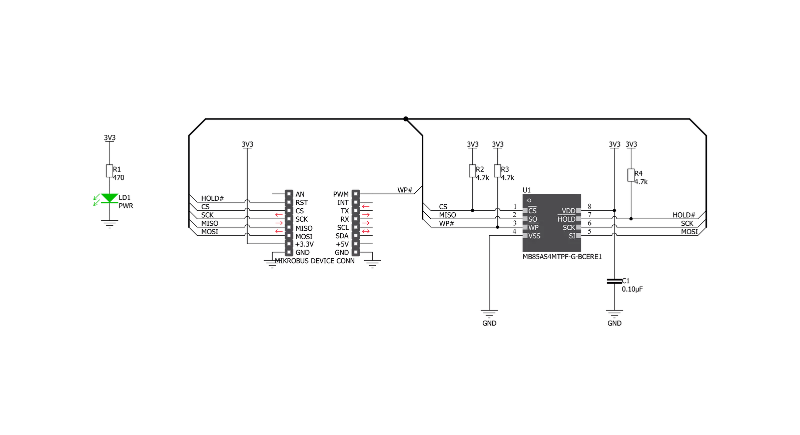
ReRAM Click board is based on the MB85AS4MT, a 4Mb serial SPI ReRAM memory module from Fujitsu. This module contains 524.288 x 8 bits of memory that can be randomly accessed. The pinout of the used memory module is the same as most commonly used EEPROM modules so that it can directly replace it. The usual SPI lines - SO, SI, SCK and #CS pins from the MB85AS4MT IC are routed to the mikroBUS™ SPI port (MISO, MOSI, SCK and CS pins). Besides the SPI serial bus, there are two more pins routed to the mikroBUS™. The #HOLD pin of the MB85AS4MT IC is routed to the RST pin of the mikroBUS™ and it is used to hold the data transfer. When this pin is pulled to a LOW logic level, all data transfer operations are suspended. However, this function is enabled only when the device is already addressed with the CS
pin pulled to a LOW level. This allows to pause the data transfer and resume it later without the need to first address it via the CS pin, reducing the output latency that way. While the data transfer is paused, the SO pin will switch to a high impedance mode (HIGH Z) and will remain inactive. The SCK pulses are completely ignored. The #HOLD pin of the MB85AS4MT IC is pulled to a HIGH logic level by an onboard pull-up resistor. The #WP pin of the MB85AS4MT IC is routed to the PWM pin of the mikroBUS™ and it is used to prevent writes to the status register, acting as a hardware write protect pin. It is routed to the RST pin of the mikroBUS™. The logical organization of the module, such as read and write commands and the status register of the MB85AS4MT IC are the same as with most commonly used
EEPROM modules, such as the one used in EEPROM 4 click. That allows this memory module, as well as ReRAM click to replace the existing EEPROM module with not too much additional work. The provided libraries offer all the functions needed to work with the ReRAM click. Their usage is demonstrated in the included example application which can be used as a reference for further development. This Click board™ can be operated only with a 3.3V logic voltage level. The board must perform appropriate logic voltage level conversion before using MCUs with different logic levels. Also, it comes equipped with a library containing functions and an example code that can be used as a reference for further development.


Features overview
Development board
Arduino UNO is a versatile microcontroller board built around the ATmega328P chip. It offers extensive connectivity options for various projects, featuring 14 digital input/output pins, six of which are PWM-capable, along with six analog inputs. Its core components include a 16MHz ceramic resonator, a USB connection, a power jack, an
ICSP header, and a reset button, providing everything necessary to power and program the board. The Uno is ready to go, whether connected to a computer via USB or powered by an AC-to-DC adapter or battery. As the first USB Arduino board, it serves as the benchmark for the Arduino platform, with "Uno" symbolizing its status as the
first in a series. This name choice, meaning "one" in Italian, commemorates the launch of Arduino Software (IDE) 1.0. Initially introduced alongside version 1.0 of the Arduino Software (IDE), the Uno has since become the foundational model for subsequent Arduino releases, embodying the platform's evolution.

Microcontroller Overview
MCU Card / MCU

Architecture
AVR
MCU Memory (KB)
32
Silicon Vendor
Microchip
Pin count
28
RAM (Bytes)
2048
You complete me!
Accessories
Click Shield for Arduino UNO has two proprietary mikroBUS™ sockets, allowing all the Click board™ devices to be interfaced with the Arduino UNO board without effort. The Arduino Uno, a microcontroller board based on the ATmega328P, provides an affordable and flexible way for users to try out new concepts and build prototypes with the ATmega328P microcontroller from various combinations of performance, power consumption, and features. The Arduino Uno has 14 digital input/output pins (of which six can be used as PWM outputs), six analog inputs, a 16 MHz ceramic resonator (CSTCE16M0V53-R0), a USB connection, a power jack, an ICSP header, and reset button. Most of the ATmega328P microcontroller pins are brought to the IO pins on the left and right edge of the board, which are then connected to two existing mikroBUS™ sockets. This Click Shield also has several switches that perform functions such as selecting the logic levels of analog signals on mikroBUS™ sockets and selecting logic voltage levels of the mikroBUS™ sockets themselves. Besides, the user is offered the possibility of using any Click board™ with the help of existing bidirectional level-shifting voltage translators, regardless of whether the Click board™ operates at a 3.3V or 5V logic voltage level. Once you connect the Arduino UNO board with our Click Shield for Arduino UNO, you can access hundreds of Click boards™, working with 3.3V or 5V logic voltage levels.

Used MCU Pins
mikroBUS™ mapper
Take a closer look
Click board™ Schematic
Step by step
Project assembly

Start by selecting your development board and Click board™. Begin with the Arduino UNO Rev3 as your development board.


Software Support
Library Description
This library contains API for ReRAM Click driver.
Key functions:
reram_send_cmd- Command Send functionreram_read_status- Status Read functionreram_write_memory- Memory Write function
Open Source
Code example
The complete application code and a ready-to-use project are available through the NECTO Studio Package Manager for direct installation in the NECTO Studio. The application code can also be found on the MIKROE GitHub account.
/*!
 * \file main.c
 * \brief ReRAM Click example
 *
 * # Description
 * This example demonstrates the use of the ReRAM Click board.
 *
 * The demo application is composed of two sections :
 *
 * ## Application Init
 * Initializes SPI serial interface and puts a device to the initial state.
 * Data from 0 to 255 will be written in memory block from address 0x0 to
 * address 0xFF.
 *
 * ## Application Task
 * Reads same memory block starting from address 0x0 to address 0xFF and
 * sends memory content to USB UART, to verify memory write operation.
 *
 * *note:*
 * Write Enable Latch is reset after the following operations:
 *  - After 'Write Disable'command recognition.
 *  - The end of writing process after 'Write Status' command recognition.
 *  - The end of writing process after 'Write Memory' command recognition.
 *
 * Data will not be written in the protected blocks of the ReRAM array.
 *  - Upper 1/4 goes from address 0x60000 to 0x7FFFF.
 *  - Upper 1/2 goes from address 0x40000 to 0x7FFFF.
 *  - The entire ReRAM array goes from address 0x00000 to 0x7FFFF.
 *
 * \author Nemanja Medakovic
 *
 */
// ------------------------------------------------------------------- INCLUDES

#include "board.h"
#include "log.h"
#include "reram.h"


// ------------------------------------------------------------------ VARIABLES

static reram_t reram;
static log_t logger;

static char write_buf[  ] = "MikroE";
static char read_buf[ 10 ] = { 0 };

// ------------------------------------------------------ APPLICATION FUNCTIONS

void application_init( void )
{
    reram_cfg_t reram_cfg;
    log_cfg_t logger_cfg;

    //  Click object initialization.
    reram_cfg_setup( &reram_cfg );
    RERAM_MAP_MIKROBUS( reram_cfg, MIKROBUS_1 );
    reram_init( &reram, &reram_cfg );

    //  Click start configuration.
    reram_default_cfg( &reram );

    /**
     * Logger initialization.
     * Default baud rate: 115200
     * Default log level: LOG_LEVEL_DEBUG
     * @note If USB_UART_RX and USB_UART_TX
     * are defined as HAL_PIN_NC, you will
     * need to define them manually for log to work.
     * See @b LOG_MAP_USB_UART macro definition for detailed explanation.
     */
    LOG_MAP_USB_UART( logger_cfg );
    log_init( &logger, &logger_cfg );

    reram_wake_up( &reram );

    uint32_t id_data = reram_read_id( &reram );

    if ( RERAM_ID_DATA != id_data )
    {
        log_printf( &logger, "***  ReRAM Error ID  ***\r\n" );
        for( ; ; );
    }
    else
    {
        log_printf( &logger, "***  ReRAM Initialization Done  ***\r\n" );
        log_printf( &logger, "***********************************\r\n" );
    }


    reram_send_cmd( &reram, RERAM_CMD_WREN );
    Delay_ms ( 1000 );
}

void application_task( void )
{
    log_printf( &logger, "* Writing data *\r\n" );

    reram_write_memory( &reram, RERAM_MEM_ADDR_START, write_buf, 6 );
    Delay_ms ( 1000 );
    reram_read_memory( &reram, RERAM_MEM_ADDR_START, read_buf, 6 );

    log_printf( &logger, "* Read data:%s\r\n", read_buf );
    Delay_ms ( 1000 );
    Delay_ms ( 1000 );
}

int main ( void )
{
    /* Do not remove this line or clock might not be set correctly. */
    #ifdef PREINIT_SUPPORTED
    preinit();
    #endif

    application_init( );

    for ( ; ; )
    {
        application_task( );
    }

    return 0;
}

// ------------------------------------------------------------------------ END
Additional Support
Resources
Category:ReRAM