Unlock the full potential of PWM with LTC8500 and STM32F031K6
48 channels, 1 SPI connection - Unleash your creativity!

Published Oct 01, 2024
Click board™
PWM 2 Click
Dev. board
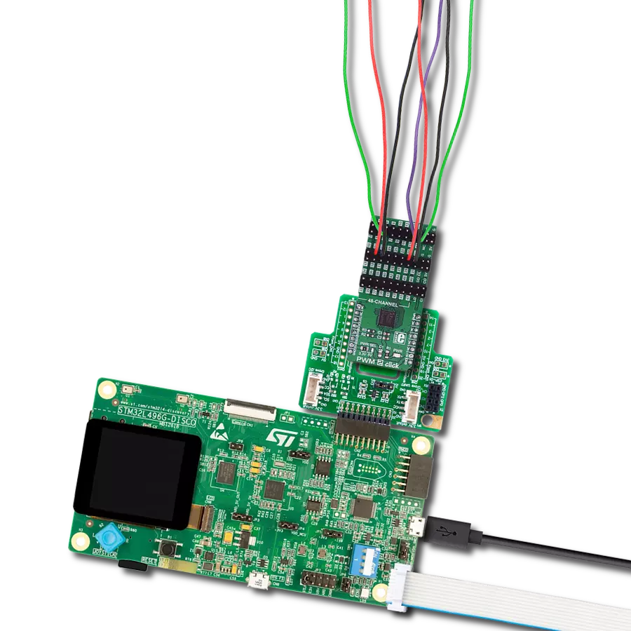
Nucleo 32 with STM32F031K6 MCU
Compiler
NECTO Studio
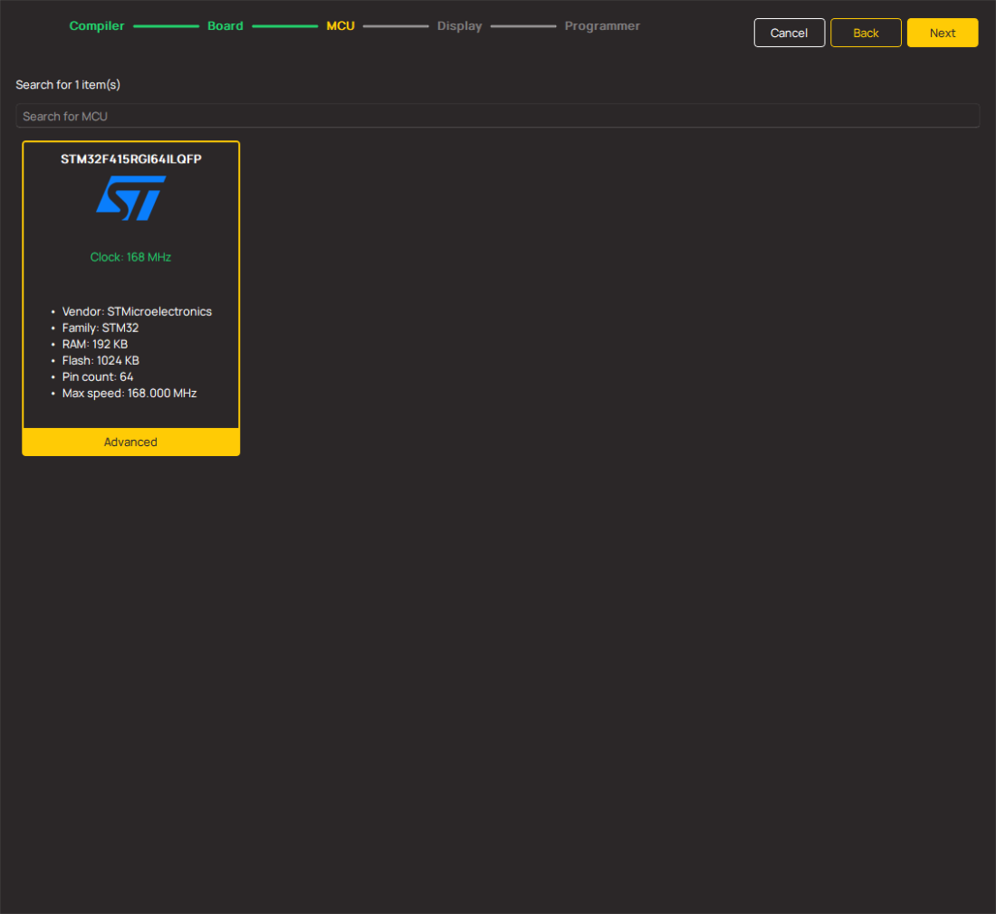
MCU
STM32F031K6
With 48 channels controlled through one interface, you gain total PWM dominance, giving you the power to manage your devices and applications with precision and efficiency
A
A
Hardware Overview
How does it work?
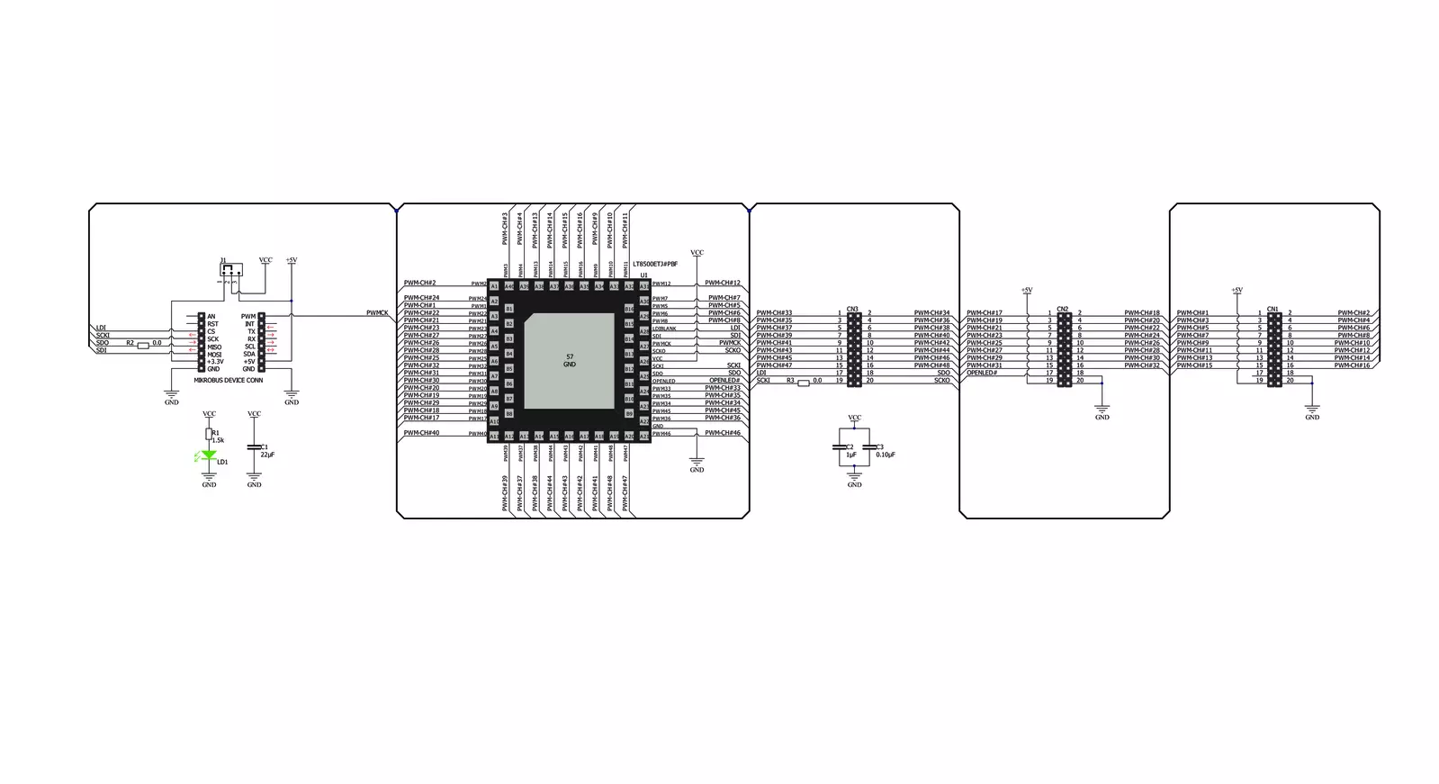
PWM 2 Click is based on the LT8500, a 48-channel LED PWM generator with 12-bit resolution and 50MHz serial interface from Analog Devices. This IC has 48 independent 12-bit PWM channels, each with 6-bit correction up to 50% of the original duty cycle. The LT8500 IC is clocked by a clock signal at the PWMCK pin. The frequency of the clock signal can go up to 25MHz, generating the PWM output frequency of up to 6.1kHz, which is sufficient for most purposes. The maximum speed of the LT8500 serial interface goes up to 50MHz in theory, but in practice, it will depend on many factors. The clock signal at the PWM pin of the mikroBUS™ is triggering an internal counter register (PWMCK). This register is compared with the content of the PWMRSYNC register, associated with each channel. Whenever the counter value is less than the value written in a specific channel PWMRSYNC register, the PWM output of that channel goes to a HIGH logic level. The frequency of the output PWM signal is therefore determined by the frequency the clock signal at the PWMCK pin. This represents the basic operating principle of the LTC8500 IC. The PWMCK pin is routed to the PWM pin of the mikroBUS™. The device uses an industry-standard SPI interface for the communication. The LDI pin acts as the normal Chip Select, latching the SPI data in, but it has an additional function if held to a HIGH logic level
for more than 50µs. In that case, the IC will be reset, and all outputs will be blanked. Therefore, care should be taken not to hold this pin to a HIGH logic level, for more than 5µs. The LDI pin is routed to the CS pin of the mikroBUS™ and it is labeled as LDI. Besides the usual SPI interface lines, the LT8500 PWM generator IC provides a serial interface clock output signal (SCKO), allowing additional devices to be connected in the parallel 5-wire topology (LDI, SCKI, SDI, SDO, and SCKO). This allows large-scale cascading, without the need for the skew balancing or buffering the signals. These additional pins are available at the standard 2.54 pitch headers on board. These additional pins on the header are described in a table, below. More information about cascading and using the SCKO feature of the IC can be found in the LT8500 datasheet. The device is controlled by sending commands via the SPI interface, embedded in a command frame. There are eight different commands which are used to control the following parameters: PWM outputs update (synchronously or asynchronously to PWM period), the dot correction factor, self-test initialization, phase shifting between banks (groups of 16 channels), enabling/ disabling of the PWM output drivers, and enabling/disabling of the dot correction . A frame consists of a 12-bit data field for each of the 48 PWM channels, followed by an
8-bit command field, which contains one of the eight command codes. The status frame is clocked on the SDO pin, providing the host MCU with the frame information: LED fault status, phase shifting status, correction status, synchronization status, and so on. This information can be used either for troubleshooting or for other purposes by the host MCU application. As already mentioned, additional functionalities of the LT8500 IC are offered via the onboard headers, along with the 48 PWM channel outputs. The outputs are not meant to drive devices with high current, so PWM 2 click is best used as the driver for additional circuitry, whether it is a simple MOSFET LED driver, or a more complex ICs, such as the LT3595A LED driver, for which a special input pin is reserved, allowing open LED conditions to be detected, even on the externally connected LT3595 IC. Onboard headers also offer fixed 5V output from the mikroBUS™ for the auxiliary purposes. This Click board™ can operate with either 3.3V or 5V logic voltage levels selected via the PWR SEL jumper. This way, both 3.3V and 5V capable MCUs can use the communication lines properly. Also, this Click board™ comes equipped with a library containing easy-to-use functions and an example code that can be used as a reference for further development.


Features overview
Development board
Nucleo 32 with STM32F031K6 MCU board provides an affordable and flexible platform for experimenting with STM32 microcontrollers in 32-pin packages. Featuring Arduino™ Nano connectivity, it allows easy expansion with specialized shields, while being mbed-enabled for seamless integration with online resources. The
board includes an on-board ST-LINK/V2-1 debugger/programmer, supporting USB reenumeration with three interfaces: Virtual Com port, mass storage, and debug port. It offers a flexible power supply through either USB VBUS or an external source. Additionally, it includes three LEDs (LD1 for USB communication, LD2 for power,
and LD3 as a user LED) and a reset push button. The STM32 Nucleo-32 board is supported by various Integrated Development Environments (IDEs) such as IAR™, Keil®, and GCC-based IDEs like AC6 SW4STM32, making it a versatile tool for developers.

Microcontroller Overview
MCU Card / MCU

Architecture
ARM Cortex-M0
MCU Memory (KB)
32
Silicon Vendor
STMicroelectronics
Pin count
32
RAM (Bytes)
4096
You complete me!
Accessories
Click Shield for Nucleo-32 is the perfect way to expand your development board's functionalities with STM32 Nucleo-32 pinout. The Click Shield for Nucleo-32 provides two mikroBUS™ sockets to add any functionality from our ever-growing range of Click boards™. We are fully stocked with everything, from sensors and WiFi transceivers to motor control and audio amplifiers. The Click Shield for Nucleo-32 is compatible with the STM32 Nucleo-32 board, providing an affordable and flexible way for users to try out new ideas and quickly create prototypes with any STM32 microcontrollers, choosing from the various combinations of performance, power consumption, and features. The STM32 Nucleo-32 boards do not require any separate probe as they integrate the ST-LINK/V2-1 debugger/programmer and come with the STM32 comprehensive software HAL library and various packaged software examples. This development platform provides users with an effortless and common way to combine the STM32 Nucleo-32 footprint compatible board with their favorite Click boards™ in their upcoming projects.

Used MCU Pins
mikroBUS™ mapper
Take a closer look
Click board™ Schematic
Step by step
Project assembly

Start by selecting your development board and Click board™. Begin with the Nucleo 32 with STM32F031K6 MCU as your development board.


Track your results in real time
Application Output
1. Application Output - In Debug mode, the 'Application Output' window enables real-time data monitoring, offering direct insight into execution results. Ensure proper data display by configuring the environment correctly using the provided tutorial.

2. UART Terminal - Use the UART Terminal to monitor data transmission via a USB to UART converter, allowing direct communication between the Click board™ and your development system. Configure the baud rate and other serial settings according to your project's requirements to ensure proper functionality. For step-by-step setup instructions, refer to the provided tutorial.

3. Plot Output - The Plot feature offers a powerful way to visualize real-time sensor data, enabling trend analysis, debugging, and comparison of multiple data points. To set it up correctly, follow the provided tutorial, which includes a step-by-step example of using the Plot feature to display Click board™ readings. To use the Plot feature in your code, use the function: plot(*insert_graph_name*, variable_name);. This is a general format, and it is up to the user to replace 'insert_graph_name' with the actual graph name and 'variable_name' with the parameter to be displayed.

Software Support
Library Description
This library contains API for PWM 2 Click driver.
Key functions:
pwm2_set_channel- Set channel function.pwm2_pwm_start- Start PWM module.send_output_enable_frame- Enable frame.
Open Source
Code example
The complete application code and a ready-to-use project are available through the NECTO Studio Package Manager for direct installation in the NECTO Studio. The application code can also be found on the MIKROE GitHub account.
/*!
 * \file
 * \brief Pwm2 Click example
 *
 * # Description
 * This application send the PWM signal in one or more outputs.
 *
 * The demo application is composed of two sections :
 *
 * ## Application Init
 * Configures the Click board and sets all PWM channels on the Click board to
 * 50% duty cycle with the phase shift enabled.
 *
 * ## Application Task
 * The first 10 PWM channels of PWM2 Click board are switched back and forth
 * from 25% duty cycle to 75% duty cycle every 10 seconds.
 *
 * \author MikroE Team
 *
 */
// ------------------------------------------------------------------- INCLUDES

#include "board.h"
#include "pwm2.h"

// ------------------------------------------------------------------ VARIABLES

static pwm2_t pwm2;

void application_init ( void )
{
    pwm2_cfg_t cfg;

    //  Click initialization.

    pwm2_cfg_setup( &cfg );
    PWM2_MAP_MIKROBUS( cfg, MIKROBUS_1 );
    pwm2_init( &pwm2, &cfg );

    pwm2_set_duty_cycle( &pwm2, 0.5 );
    pwm2_pwm_start( &pwm2 );

    pwm2_default_cfg( &pwm2 );
    pwm2_toggle_phase_shift( &pwm2 );

    //setting all 48 PWM channels of the PWM2 Click to 50% duty
    for( uint8_t cnt = 1; cnt < 49; cnt++ )
    {
        pwm2_set_channel( &pwm2, cnt, PWM2_50_PERCENT_DUTY, PWM2_NO_CORRECTION );
    }
}

void application_task ( void )
{
    for ( uint8_t cnt = 1; cnt < 10; cnt++ )
    {
        pwm2_set_channel( &pwm2, cnt, PWM2_25_PERCENT_DUTY, PWM2_NO_CORRECTION );
    }
    // 10 seconds delay
    Delay_ms ( 1000 );
    Delay_ms ( 1000 );
    Delay_ms ( 1000 );
    Delay_ms ( 1000 );
    Delay_ms ( 1000 );
    Delay_ms ( 1000 );
    Delay_ms ( 1000 );
    Delay_ms ( 1000 );
    Delay_ms ( 1000 );
    Delay_ms ( 1000 );

    for ( uint8_t cnt = 1; cnt < 10; cnt++ )
    {
        pwm2_set_channel( &pwm2, cnt, PWM2_75_PERCENT_DUTY, PWM2_NO_CORRECTION );
    }
    // 10 seconds delay
    Delay_ms ( 1000 );
    Delay_ms ( 1000 );
    Delay_ms ( 1000 );
    Delay_ms ( 1000 );
    Delay_ms ( 1000 );
    Delay_ms ( 1000 );
    Delay_ms ( 1000 );
    Delay_ms ( 1000 );
    Delay_ms ( 1000 );
    Delay_ms ( 1000 );
}

int main ( void )
{
    /* Do not remove this line or clock might not be set correctly. */
    #ifdef PREINIT_SUPPORTED
    preinit();
    #endif

    application_init( );

    for ( ; ; )
    {
        application_task( );
    }

    return 0;
}


// ------------------------------------------------------------------------ END
Additional Support
Resources
Category:PWM