Add DRAM memory to your design with APS6404L-3SQR and STM32F407VGT6
Put your memory to good use!

Published Mar 11, 2023
Click board™
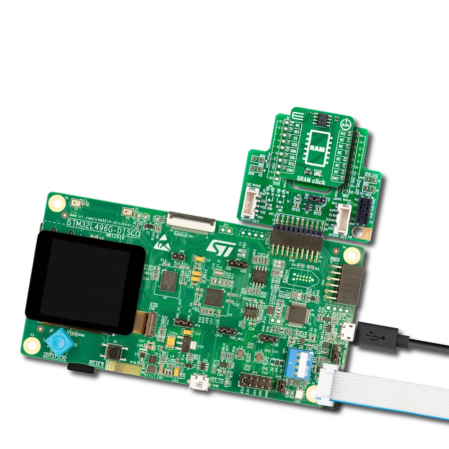
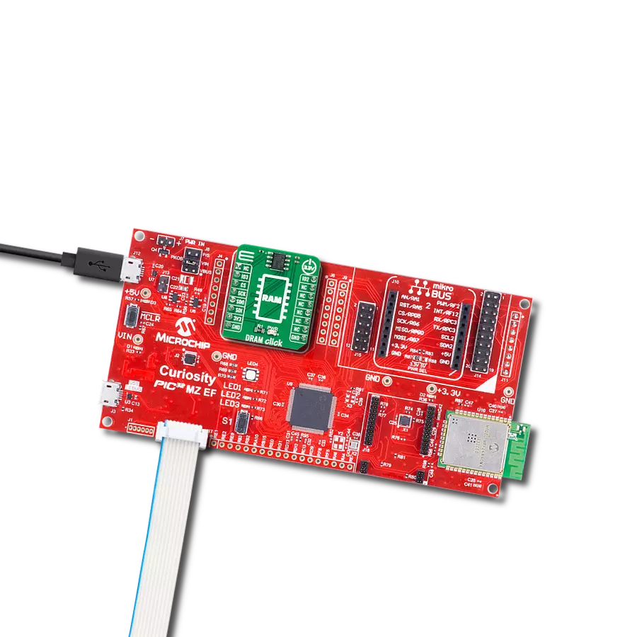
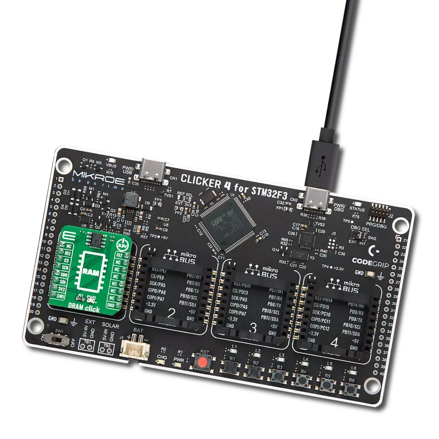
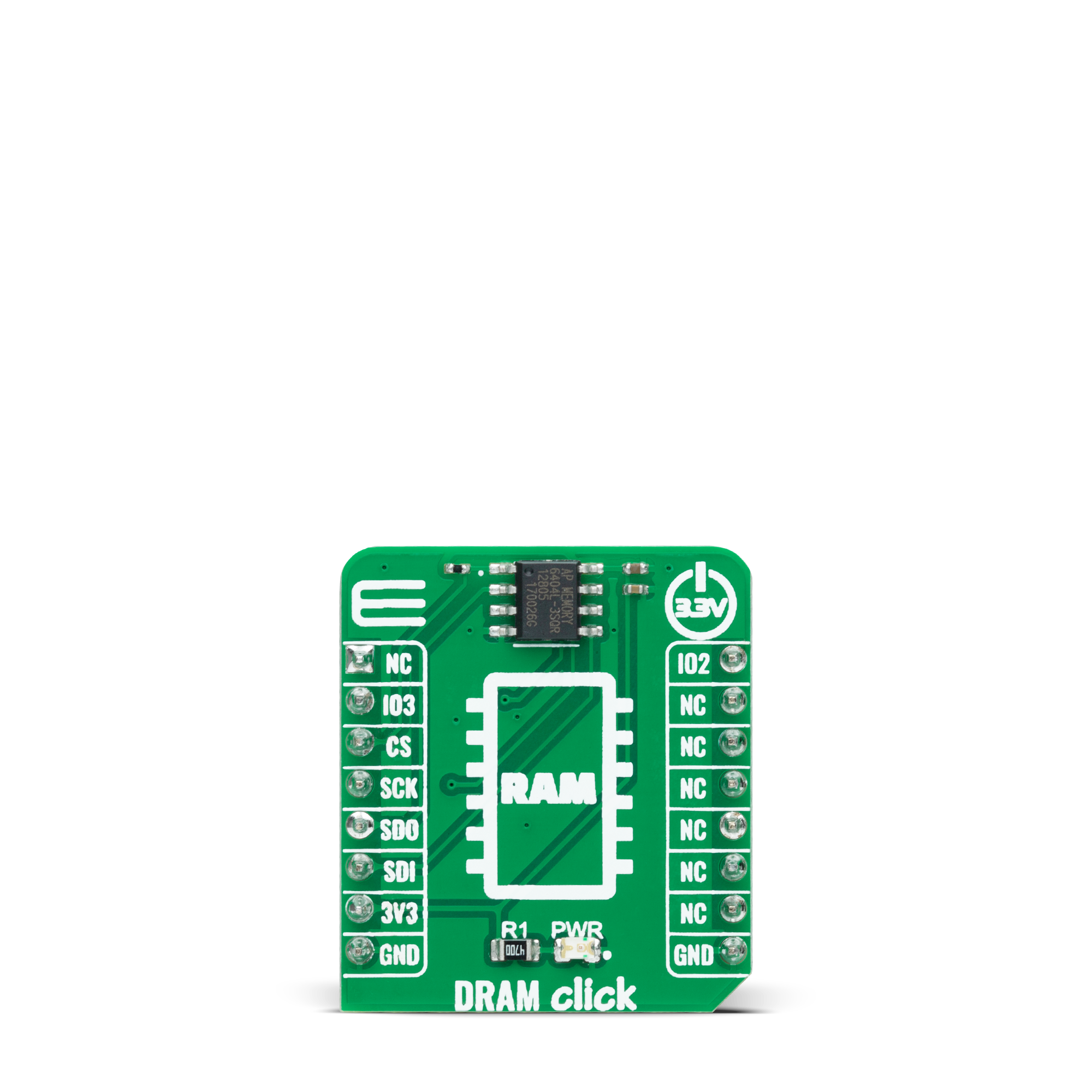
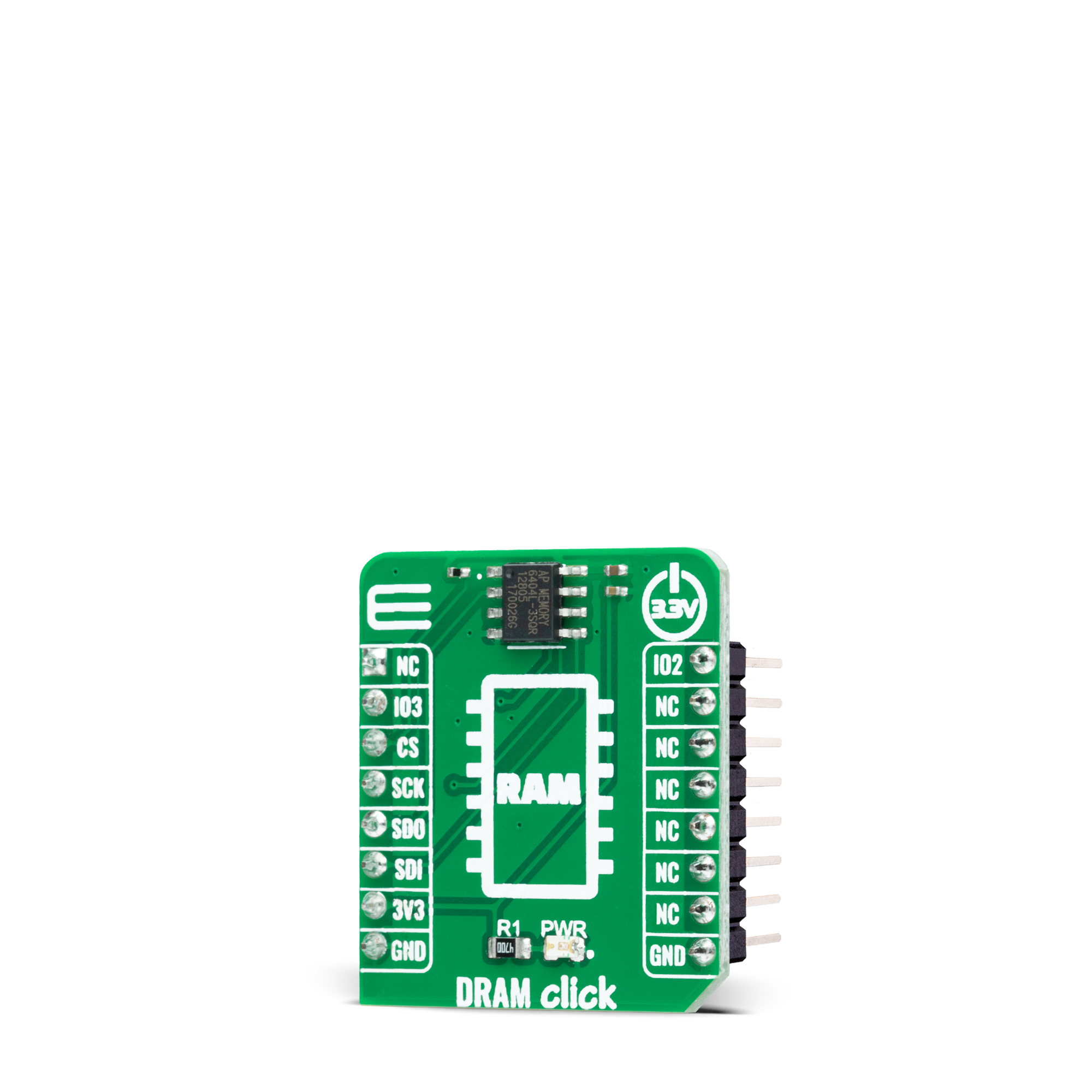
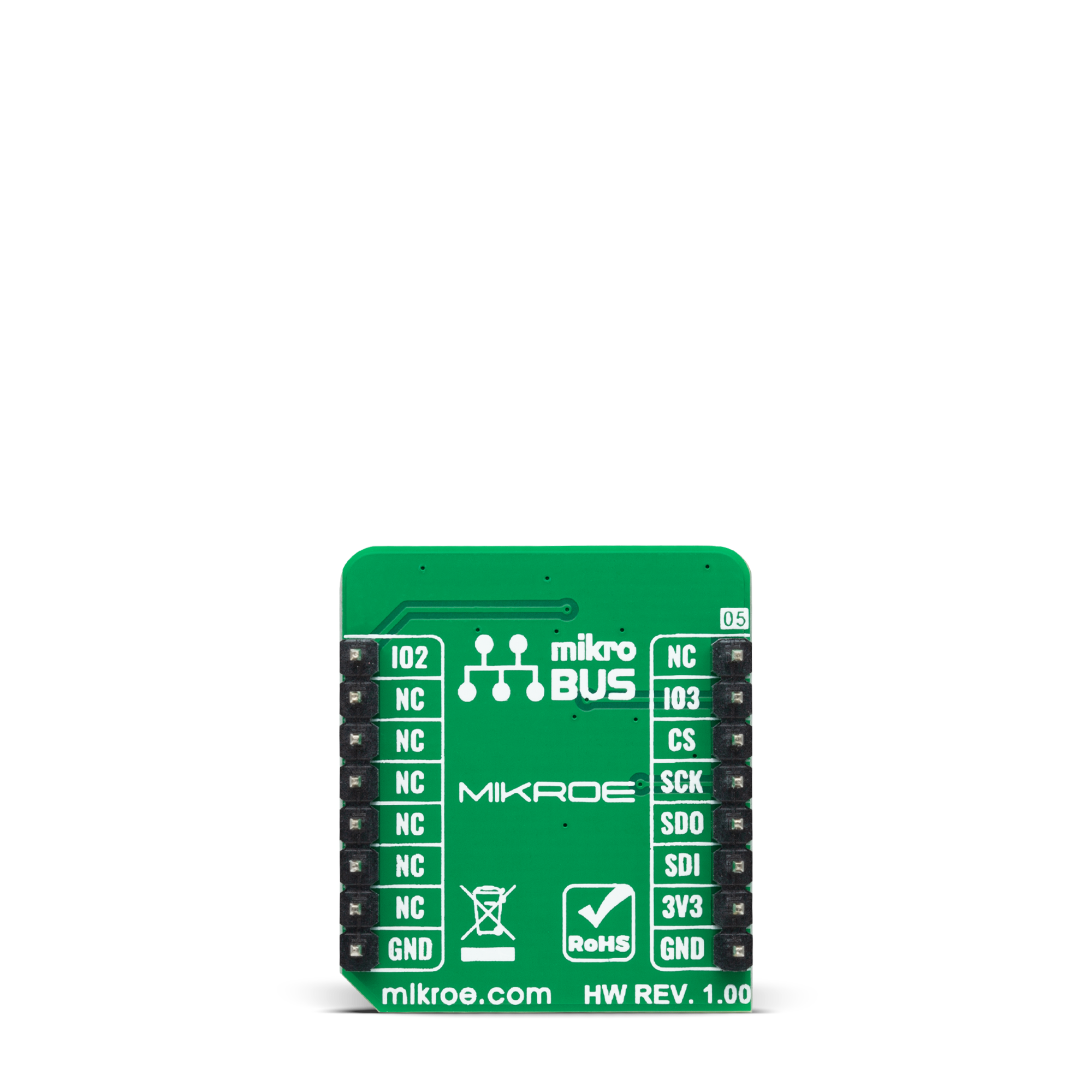
DRAM Click
Dev. board
Clicker 2 for STM32
Compiler
NECTO Studio
MCU
STM32F407VGT6
Secure your information with a quality DRAM memory
A
A
Hardware Overview
How does it work?
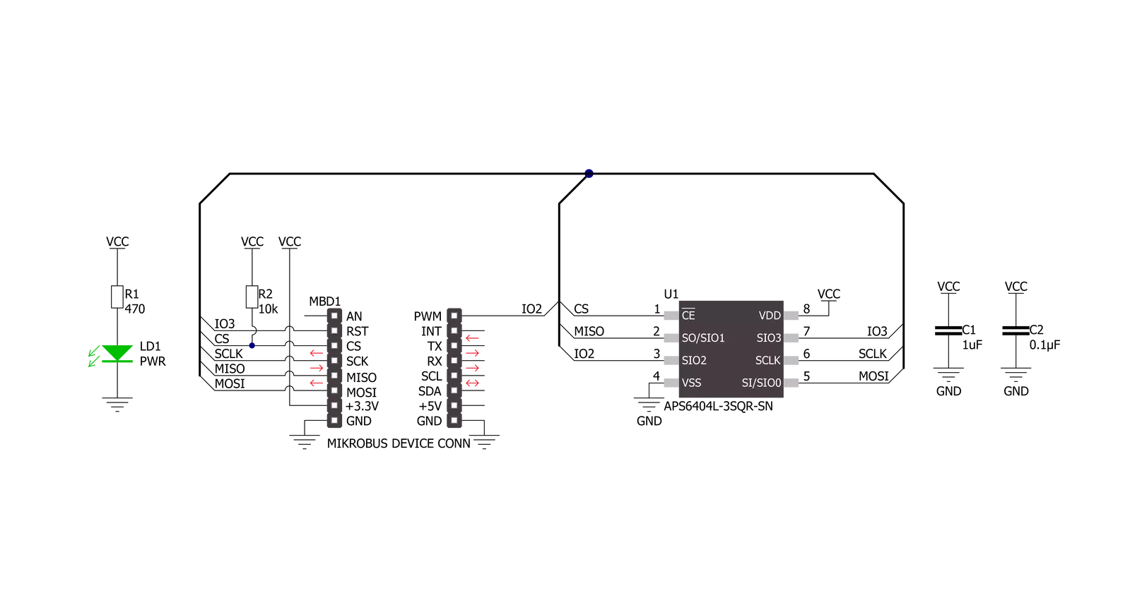
DRAM Click is based on the APS6404L-3SQR, a 64Mb PSRAM (Pseudo-SRAM) memory with an SPI/QPI interface from AP Memory. Organized as 8M x 8 bits each, this high-speed, high-performance memory has a page size of 1024 bytes. It also incorporates a seamless, self-managed refresh mechanism specially designed to maximize the performance of the memory read operation (it does not require the support of DRAM refresh from the system host). It is most suitable for low-power and low-cost portable applications.
The APS6404L-3SQR communicates with the MCU using an SPI serial interface that also supports Quad SPI and the two most common modes, SPI Mode 0 (QSPI Mode 1), with a maximum SPI frequency of 133MHz. The APS6404L-3SQR includes an on-chip voltage sensor used to start the self-initialization process. When the main power supply voltage reaches a stable level at or above the minimum supply voltage level, the device will require 150μs and user-issued RESET Operation to complete its self-initialization
process. The device powers up in SPI mode by default but can also switch to QPI mode. The CS pin must be set to high logic level before initiating any operations. This Click board™ can only be operated with a 3.3V logic voltage level. The board must perform appropriate logic voltage level conversion before using MCUs with different logic levels. However, the Click board™ comes equipped with a library containing functions and an example code that can be used as a reference for further development.
Features overview
Development board
Clicker 2 for STM32 is a compact starter development board that brings the flexibility of add-on Click boards™ to your favorite microcontroller, making it a perfect starter kit for implementing your ideas. It comes with an onboard 32-bit ARM Cortex-M4 microcontroller, the STM32F407VGT6 from STMicroelectronics, two mikroBUS™ sockets for Click board™ connectivity, a USB connector, LED indicators, buttons, a JTAG programmer connector, and two 26-pin headers for interfacing with external electronics. Its compact design with clear and easily recognizable silkscreen markings allows you to build gadgets with unique functionalities and features quickly. Each part of the Clicker 2 for
STM32 development kit contains the components necessary for the most efficient operation of the same board. In addition to the possibility of choosing the Clicker 2 for STM32 programming method, using a USB HID mikroBootloader, an external mikroProg connector for STM32 programmer, or through an external ST-LINK V2 programmer, the Clicker 2 board also includes a clean and regulated power supply module for the development kit. It provides two ways of board-powering; through the USB Mini-B cable, where onboard voltage regulators provide the appropriate voltage levels to each component on the board or using a Li-Polymer battery via an onboard battery
connector. All communication methods that mikroBUS™ itself supports are on this board, including the well-established mikroBUS™ socket, reset button, and several user-configurable buttons and LED indicators. Clicker 2 for STM32 is an integral part of the Mikroe ecosystem, allowing you to create a new application in minutes. Natively supported by Mikroe software tools, it covers many aspects of prototyping thanks to a considerable number of different Click boards™ (over a thousand boards), the number of which is growing every day.

Microcontroller Overview
MCU Card / MCU
Architecture
ARM Cortex-M4
MCU Memory (KB)
10
Silicon Vendor
STMicroelectronics
Pin count
100
RAM (Bytes)
100
Used MCU Pins
mikroBUS™ mapper
Take a closer look
Click board™ Schematic
Step by step
Project assembly

Start by selecting your development board and Click board™. Begin with the Clicker 2 for STM32 as your development board.


Track your results in real time
Application Output
1. Application Output - In Debug mode, the 'Application Output' window enables real-time data monitoring, offering direct insight into execution results. Ensure proper data display by configuring the environment correctly using the provided tutorial.

2. UART Terminal - Use the UART Terminal to monitor data transmission via a USB to UART converter, allowing direct communication between the Click board™ and your development system. Configure the baud rate and other serial settings according to your project's requirements to ensure proper functionality. For step-by-step setup instructions, refer to the provided tutorial.

3. Plot Output - The Plot feature offers a powerful way to visualize real-time sensor data, enabling trend analysis, debugging, and comparison of multiple data points. To set it up correctly, follow the provided tutorial, which includes a step-by-step example of using the Plot feature to display Click board™ readings. To use the Plot feature in your code, use the function: plot(*insert_graph_name*, variable_name);. This is a general format, and it is up to the user to replace 'insert_graph_name' with the actual graph name and 'variable_name' with the parameter to be displayed.

Software Support
Library Description
This library contains API for DRAM Click driver.
Key functions:
dram_memory_writeThis function writes a desired number of data bytes starting from the selected memory address.dram_memory_readThis function reads a desired number of data bytes starting from the selected memory address.dram_memory_read_fastThis function reads a desired number of data bytes starting from the selected memory address performing a fast read feature.
Open Source
Code example
The complete application code and a ready-to-use project are available through the NECTO Studio Package Manager for direct installation in the NECTO Studio. The application code can also be found on the MIKROE GitHub account.
/*!
 * @file main.c
 * @brief DRAM Click example
 *
 * # Description
 * This example demonstrates the use of DRAM Click board by writing specified data to
 * the memory and reading it back.
 *
 * The demo application is composed of two sections :
 *
 * ## Application Init
 * Initializes the driver, resets the device and checks the communication by reading
 * and verifying the device ID.
 *
 * ## Application Task
 * Writes a desired number of bytes to the memory and then verifies if it is written correctly
 * by reading from the same memory location and displaying the memory content on the USB UART.
 *
 * @author Stefan Filipovic
 *
 */

#include "board.h"
#include "log.h"
#include "dram.h"

#define DEMO_TEXT_MESSAGE_1     "MikroE"
#define DEMO_TEXT_MESSAGE_2     "DRAM Click"
#define STARTING_ADDRESS        0x012345ul

static dram_t dram;
static log_t logger;

void application_init ( void )
{
    log_cfg_t log_cfg;  /**< Logger config object. */
    dram_cfg_t dram_cfg;  /**< Click config object. */

    /**
     * Logger initialization.
     * Default baud rate: 115200
     * Default log level: LOG_LEVEL_DEBUG
     * @note If USB_UART_RX and USB_UART_TX
     * are defined as HAL_PIN_NC, you will
     * need to define them manually for log to work.
     * See @b LOG_MAP_USB_UART macro definition for detailed explanation.
     */
    LOG_MAP_USB_UART( log_cfg );
    log_init( &logger, &log_cfg );
    log_info( &logger, " Application Init " );

    // Click initialization.
    dram_cfg_setup( &dram_cfg );
    DRAM_MAP_MIKROBUS( dram_cfg, MIKROBUS_1 );
    if ( SPI_MASTER_ERROR == dram_init( &dram, &dram_cfg ) )
    {
        log_error( &logger, " Communication init." );
        for ( ; ; );
    }

    if ( DRAM_ERROR == dram_reset ( &dram ) )
    {
        log_error( &logger, " Reset device." );
        for ( ; ; );
    }
    Delay_ms ( 100 );

    if ( DRAM_ERROR == dram_check_communication ( &dram ) )
    {
        log_error( &logger, " Check communication." );
        for ( ; ; );
    }

    log_info( &logger, " Application Task " );
}

void application_task ( void )
{
    uint8_t data_buf[ 128 ] = { 0 };
    log_printf ( &logger, " Memory address: 0x%.6LX\r\n", ( uint32_t ) STARTING_ADDRESS );
    memcpy ( data_buf, DEMO_TEXT_MESSAGE_1, strlen ( DEMO_TEXT_MESSAGE_1 ) );
    if ( DRAM_OK == dram_memory_write ( &dram, STARTING_ADDRESS, data_buf, sizeof ( data_buf ) ) )
    {
        log_printf ( &logger, " Write data: %s\r\n", data_buf );
        Delay_ms ( 100 );
    }
    memset ( data_buf, 0, sizeof ( data_buf ) );
    if ( DRAM_OK == dram_memory_read ( &dram, STARTING_ADDRESS,
                                             data_buf, sizeof ( data_buf ) ) )
    {
        log_printf ( &logger, " Read data: %s\r\n\n", data_buf );
        Delay_ms ( 1000 );
        Delay_ms ( 1000 );
        Delay_ms ( 1000 );
    }
    log_printf ( &logger, " Memory address: 0x%.6LX\r\n", ( uint32_t ) STARTING_ADDRESS );
    memcpy ( data_buf, DEMO_TEXT_MESSAGE_2, strlen ( DEMO_TEXT_MESSAGE_2 ) );
    if ( DRAM_OK == dram_memory_write ( &dram, STARTING_ADDRESS, data_buf, sizeof ( data_buf ) ) )
    {
        log_printf ( &logger, " Write data: %s\r\n", data_buf );
        Delay_ms ( 100 );
    }
    memset ( data_buf, 0, sizeof ( data_buf ) );
    if ( DRAM_OK == dram_memory_read_fast ( &dram, STARTING_ADDRESS, data_buf, sizeof ( data_buf ) ) )
    {
        log_printf ( &logger, " Fast read data : %s\r\n\n", data_buf );
        Delay_ms ( 1000 );
        Delay_ms ( 1000 );
        Delay_ms ( 1000 );
    }
}

int main ( void )
{
    /* Do not remove this line or clock might not be set correctly. */
    #ifdef PREINIT_SUPPORTED
    preinit();
    #endif

    application_init( );

    for ( ; ; )
    {
        application_task( );
    }

    return 0;
}

// ------------------------------------------------------------------------ END