Change analog signals to digital with MAX22005 and PIC32MZ2048EFH100
Digitize your data

Published Mar 11, 2023
Click board™
ADC 18 Click
Dev. board
Flip&Click PIC32MZ
Compiler
NECTO Studio
MCU
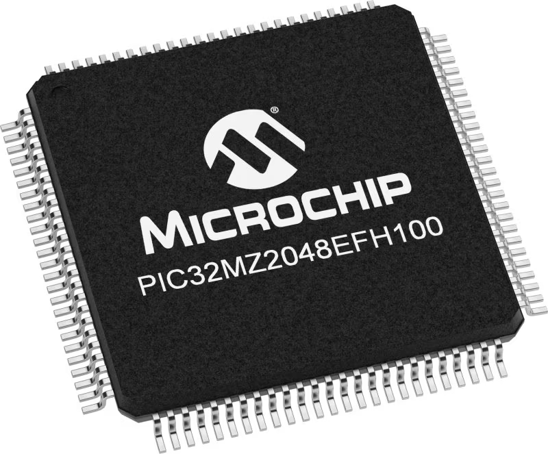
PIC32MZ2048EFH100
Translate analog signals for data processing purposes
A
A
Hardware Overview
How does it work?
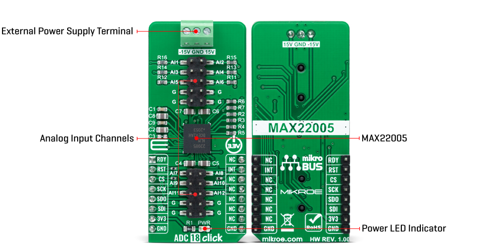
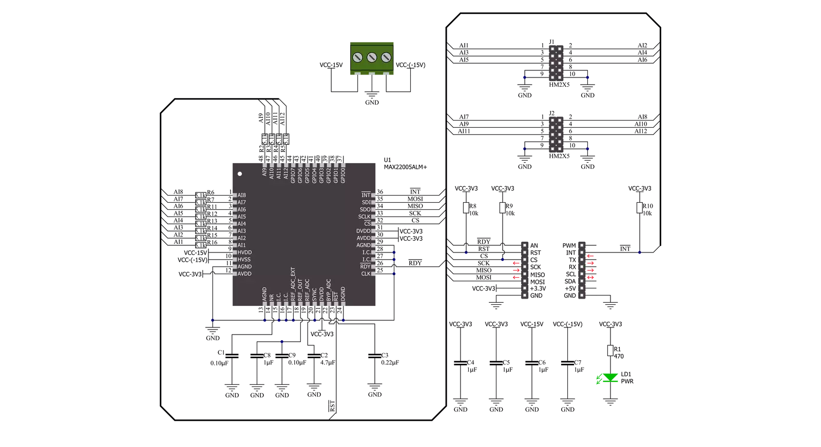
ADC 18 Click is based on the MAX22005, a high-performance twelve-channel analog-to-digital converter from Analog Devices. The MAX22005 has an integrated 24-bit delta-sigma ADC, input multiplexer, signal conditioning, and control logic block, allowing ADC to communicate with MCU through a high-speed serial interface. An integrated delta-sigma ADC is shared between all channels with an integrated 5ppm/°C precision reference. Using high-voltage, zero-drift input amplifiers, standard industrial analog input voltage ranges are converted to the ADC input voltage range. Input channels can be used as twelve single-ended, six differential, and up to eight multichannel configurable differential inputs. In total, the device supports up to 26 different configurations. The MAX22005 can also be configured as an analog-input
current-mode device using an external precision resistor per channel or configurable analog input using an external precision resistor and low-cost switch per channel. All input ports are robustly protected up to ±36V reverse polarity and ±2kV surge pulses without the need for TVS diodes and factory calibrated with a best-in-class system performance of less than 0.05% FSR Total-Unadjusted-Error (TUE) over temperature. ADC 18 Click communicates with MCU through a standard SPI interface and operates at clock rates up to 30MHz, for all configurations and information management and acquiring conversion results. In addition, it also uses several mikroBUS™ pins. An active-low reset signal routed on the RST pin of the mikroBUS™ socket activates a hardware reset of the system, while the INT pin on the mikroBUS™
socket represents a standard interrupt feature providing a user with feedback information. It also has an additional data-ready interrupt marked as RDY and routed on the AN pin of the mikroBUS™ socket, used to signal when a new ADC conversion result is available in the data register. This Click board™ can only be operated with a 3.3V logic voltage level. It also has an analog inputs external power supply terminal where it is necessary to bring ±15V to accept ± 10V inputs, whose full-scale range is ± 12.5V. The board must perform appropriate logic voltage level conversion before using MCUs with different logic levels. However, the Click board™ comes equipped with a library containing functions and an example code that can be used, as a reference, for further development.
Features overview
Development board
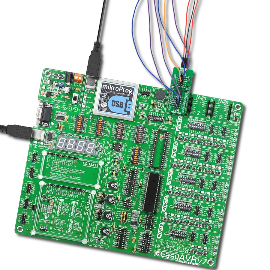
Flip&Click PIC32MZ is a compact development board designed as a complete solution that brings the flexibility of add-on Click boards™ to your favorite microcontroller, making it a perfect starter kit for implementing your ideas. It comes with an onboard 32-bit PIC32MZ microcontroller, the PIC32MZ2048EFH100 from Microchip, four mikroBUS™ sockets for Click board™ connectivity, two USB connectors, LED indicators, buttons, debugger/programmer connectors, and two headers compatible with Arduino-UNO pinout. Thanks to innovative manufacturing technology,
it allows you to build gadgets with unique functionalities and features quickly. Each part of the Flip&Click PIC32MZ development kit contains the components necessary for the most efficient operation of the same board. In addition, there is the possibility of choosing the Flip&Click PIC32MZ programming method, using the chipKIT bootloader (Arduino-style development environment) or our USB HID bootloader using mikroC, mikroBasic, and mikroPascal for PIC32. This kit includes a clean and regulated power supply block through the USB Type-C (USB-C) connector. All communication
methods that mikroBUS™ itself supports are on this board, including the well-established mikroBUS™ socket, user-configurable buttons, and LED indicators. Flip&Click PIC32MZ development kit allows you to create a new application in minutes. Natively supported by Mikroe software tools, it covers many aspects of prototyping thanks to a considerable number of different Click boards™ (over a thousand boards), the number of which is growing every day.

Microcontroller Overview
MCU Card / MCU
Architecture
PIC32
MCU Memory (KB)
2048
Silicon Vendor
Microchip
Pin count
100
RAM (Bytes)
524288
Used MCU Pins
mikroBUS™ mapper
Take a closer look
Click board™ Schematic
Step by step
Project assembly

Start by selecting your development board and Click board™. Begin with the Flip&Click PIC32MZ as your development board.


Track your results in real time
Application Output
1. Application Output - In Debug mode, the 'Application Output' window enables real-time data monitoring, offering direct insight into execution results. Ensure proper data display by configuring the environment correctly using the provided tutorial.

2. UART Terminal - Use the UART Terminal to monitor data transmission via a USB to UART converter, allowing direct communication between the Click board™ and your development system. Configure the baud rate and other serial settings according to your project's requirements to ensure proper functionality. For step-by-step setup instructions, refer to the provided tutorial.

3. Plot Output - The Plot feature offers a powerful way to visualize real-time sensor data, enabling trend analysis, debugging, and comparison of multiple data points. To set it up correctly, follow the provided tutorial, which includes a step-by-step example of using the Plot feature to display Click board™ readings. To use the Plot feature in your code, use the function: plot(*insert_graph_name*, variable_name);. This is a general format, and it is up to the user to replace 'insert_graph_name' with the actual graph name and 'variable_name' with the parameter to be displayed.

Software Support
Library Description
This library contains API for ADC 18 Click driver.
Key functions:
adc18_set_active_channelThis function sets the active channel.adc18_start_conversionThis function starts the conversion with the selected data rate.adc18_read_voltageThis function reads RAW ADC value of previous conversion and converts it to voltage.
Open Source
Code example
The complete application code and a ready-to-use project are available through the NECTO Studio Package Manager for direct installation in the NECTO Studio. The application code can also be found on the MIKROE GitHub account.
/*!
 * @file main.c
 * @brief ADC18 Click example
 *
 * # Description
 * This example demonstrates the use of ADC 18 Click board by reading
 * the voltage from 12 analog input single-ended channels.
 *
 * The demo application is composed of two sections :
 *
 * ## Application Init
 * Initializes the driver and logger, and performs the Click default configuration.
 *
 * ## Application Task
 * Reads and displays the voltage from 12 analog input single-ended channels
 * on the USB UART approximately once per second.
 *
 * @author Stefan Filipovic
 *
 */

#include "board.h"
#include "log.h"
#include "adc18.h"

static adc18_t adc18;
static log_t logger;

void application_init ( void )
{
    log_cfg_t log_cfg;  /**< Logger config object. */
    adc18_cfg_t adc18_cfg;  /**< Click config object. */

    /**
     * Logger initialization.
     * Default baud rate: 115200
     * Default log level: LOG_LEVEL_DEBUG
     * @note If USB_UART_RX and USB_UART_TX
     * are defined as HAL_PIN_NC, you will
     * need to define them manually for log to work.
     * See @b LOG_MAP_USB_UART macro definition for detailed explanation.
     */
    LOG_MAP_USB_UART( log_cfg );
    log_init( &logger, &log_cfg );
    log_info( &logger, " Application Init " );

    // Click initialization.
    adc18_cfg_setup( &adc18_cfg );
    ADC18_MAP_MIKROBUS( adc18_cfg, MIKROBUS_1 );
    if ( SPI_MASTER_ERROR == adc18_init( &adc18, &adc18_cfg ) )
    {
        log_error( &logger, " Communication init." );
        for ( ; ; );
    }

    if ( ADC18_ERROR == adc18_default_cfg ( &adc18 ) )
    {
        log_error( &logger, " Default configuration." );
        for ( ; ; );
    }

    log_info( &logger, " Application Task " );
}

void application_task ( void )
{
    static uint8_t channel = ADC18_CH_AI1_SINGLE_ENDED;
    if ( ADC18_OK == adc18_set_active_channel ( &adc18, channel ) )
    {
        adc18_start_conversion ( &adc18, ADC18_DATA_RATE_225_SPS );

        // Waits for the availability of the conversion result
        while ( adc18_get_rdy_pin ( &adc18 ) );

        adc18_stop_conversion ( &adc18 );

        float voltage;
        if ( ADC18_OK == adc18_read_voltage ( &adc18, &voltage ) )
        {
            log_printf ( &logger, "Channel AI%u: %.2f V\r\n", channel + 1, voltage );
            if ( ++channel > ADC18_CH_AI12_SINGLE_ENDED )
            {
                channel = ADC18_CH_AI1_SINGLE_ENDED;
                log_printf ( &logger, "\r\n" );
                Delay_ms ( 1000 );
            }
        }
    }
}

int main ( void )
{
    /* Do not remove this line or clock might not be set correctly. */
    #ifdef PREINIT_SUPPORTED
    preinit();
    #endif

    application_init( );

    for ( ; ; )
    {
        application_task( );
    }

    return 0;
}

// ------------------------------------------------------------------------ END