Convert multiple analog signals into digital data with MCP3204 and PIC32MZ2048EFM100
4-channel 12-bit ADC with SPI interface

Published Jan 23, 2024
Click board™
ADC Click
Dev. board
Curiosity PIC32 MZ EF
Compiler
NECTO Studio
MCU
PIC32MZ2048EFM100
Help electronics understand and work with information from the real world
A
A
Hardware Overview
How does it work?
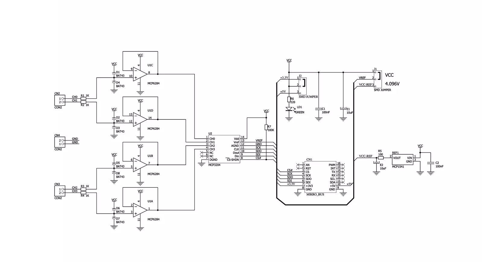
ADC Click is based on the MCP3204, a 4-channel 12-bit A/D converter with SPI serial interface from Microchip. The MCP3204 contains an input channel selection multiplexer (CH0, CH1, CH2, CH3) which for reference can use the VCC (3.3V or 5V) or a 4.096V of the MCP1541 voltage reference from Microchip. The voltage reference determines the analog voltage range and can be selected via REFERENCE onboard jumper. To connect the
analog voltages to the ADC Click, utilize the four labeled terminals CH0-3 along with two GND terminals for referencing the ground. Each analog input pin goes through the MCP6284, a 5MHz rail-to-rail OpAmp from Microchip. The ADC Click uses a standard 4-Wire SPI serial interface to communicate with the host MCU, supporting both 0 and 3 of the SPI modes and operating at clock rates of up to 2MHz. Communication with the ADC
Click is initiated by bringing the CS line LOW. This Click board™ can operate with either 3.3V or 5V logic voltage levels selected via the PWR SEL jumper. This way, both 3.3V and 5V capable MCUs can use the communication lines properly. However, the Click board™ comes equipped with a library containing easy-to-use functions and an example code that can be used, as a reference, for further development.

Features overview
Development board
Curiosity PIC32 MZ EF development board is a fully integrated 32-bit development platform featuring the high-performance PIC32MZ EF Series (PIC32MZ2048EFM) that has a 2MB Flash, 512KB RAM, integrated FPU, Crypto accelerator, and excellent connectivity options. It includes an integrated programmer and debugger, requiring no additional hardware. Users can expand
functionality through MIKROE mikroBUS™ Click™ adapter boards, add Ethernet connectivity with the Microchip PHY daughter board, add WiFi connectivity capability using the Microchip expansions boards, and add audio input and output capability with Microchip audio daughter boards. These boards are fully integrated into PIC32’s powerful software framework, MPLAB Harmony,
which provides a flexible and modular interface to application development a rich set of inter-operable software stacks (TCP-IP, USB), and easy-to-use features. The Curiosity PIC32 MZ EF development board offers expansion capabilities making it an excellent choice for a rapid prototyping board in Connectivity, IOT, and general-purpose applications.

Microcontroller Overview
MCU Card / MCU
Architecture
PIC32
MCU Memory (KB)
2048
Silicon Vendor
Microchip
Pin count
100
RAM (Bytes)
524288
Used MCU Pins
mikroBUS™ mapper
Take a closer look
Click board™ Schematic
Step by step
Project assembly

Start by selecting your development board and Click board™. Begin with the Curiosity PIC32 MZ EF as your development board.


Track your results in real time
Application Output
1. Application Output - In Debug mode, the 'Application Output' window enables real-time data monitoring, offering direct insight into execution results. Ensure proper data display by configuring the environment correctly using the provided tutorial.

2. UART Terminal - Use the UART Terminal to monitor data transmission via a USB to UART converter, allowing direct communication between the Click board™ and your development system. Configure the baud rate and other serial settings according to your project's requirements to ensure proper functionality. For step-by-step setup instructions, refer to the provided tutorial.

3. Plot Output - The Plot feature offers a powerful way to visualize real-time sensor data, enabling trend analysis, debugging, and comparison of multiple data points. To set it up correctly, follow the provided tutorial, which includes a step-by-step example of using the Plot feature to display Click board™ readings. To use the Plot feature in your code, use the function: plot(*insert_graph_name*, variable_name);. This is a general format, and it is up to the user to replace 'insert_graph_name' with the actual graph name and 'variable_name' with the parameter to be displayed.

Software Support
Library Description
This library contains API for ADC Click driver.
Key functions:
adc_get_single_ended_ch- Get Single-Ended Channel functionadc_get_differential_ch- Get Pseudo-Differential Pair function
Open Source
Code example
The complete application code and a ready-to-use project are available through the NECTO Studio Package Manager for direct installation in the NECTO Studio. The application code can also be found on the MIKROE GitHub account.
/*!
 * \file main.c
 * \brief ADC Click example
 *
 * # Description
 * This example demonstrates the use of ADC Click board.
 * The all channels can be configured as single-ended or pseudo-differential
 * pair.
 *
 * The demo application is composed of two sections :
 *
 * ## Application Init
 * Initializes SPI driver, performs the reference voltage selection and
 * initializes UART console for results logging.
 *
 * ## Application Task
 * Reads voltage level of channels 0 and 1 in the both configurations,
 * single-ended and pseudo-differential pair, every 1 second.
 * All channels results will be calculated to millivolts [mV].
 *
 * *note:*
 * In single-ended mode the all channels must be in the range from Vss (GND)
 * to Vref (3V3 by default).
 * In pseudo-differential mode the IN- channel must be in the range from
 * (Vss - 100mV) to (Vss + 100mV). The IN+ channel must be in the range from
 * IN- to (Vref + IN-).
 * If any of conditions are not fullfilled, the device will return 0 or Vref
 * voltage level, and measurements are not valid.
 *
 * \author Nemanja Medakovic
 *
 */
// ------------------------------------------------------------------- INCLUDES

#include "board.h"
#include "log.h"
#include "adc.h"


// ------------------------------------------------------------------ VARIABLES

static adc_t adc;
static log_t logger;

// ------------------------------------------------------ APPLICATION FUNCTIONS

void application_init( void )
{
    log_cfg_t log_cfg;
    adc_cfg_t cfg;

    /**
     * Logger initialization.
     * Default baud rate: 115200
     * Default log level: LOG_LEVEL_DEBUG
     * @note If USB_UART_RX and USB_UART_TX
     * are defined as HAL_PIN_NC, you will
     * need to define them manually for log to work.
     * See @b LOG_MAP_USB_UART macro definition for detailed explanation.
     */
    LOG_MAP_USB_UART( log_cfg );
    log_init( &logger, &log_cfg );
    log_info( &logger, "---- Application Init ----" );

    //  Click initialization.

    adc_cfg_setup( &cfg );
    ADC_MAP_MIKROBUS( cfg, MIKROBUS_1 );
    adc_init( &adc, &cfg );
}

void application_task( void )
{
    adc_get_single_ended_ch( &adc, ADC_CH0_OR_CH01 );
    adc_get_single_ended_ch( &adc, ADC_CH1_OR_CH10 );
    adc_get_single_ended_ch( &adc, ADC_CH2_OR_CH23 );
    adc_get_single_ended_ch( &adc, ADC_CH3_OR_CH32 );
    adc_get_differential_ch( &adc, ADC_CH0_OR_CH01 );

    log_printf( &logger, "* CH0 = %u mV\r\n", adc.ch0 );
    log_printf( &logger, "* CH1 = %u mV\r\n", adc.ch1 );
    log_printf( &logger, "* CH2 = %u mV\r\n", adc.ch2 );
    log_printf( &logger, "* CH3 = %u mV\r\n", adc.ch3 );
    log_printf( &logger, "* CH0 - CH1 = %d mV\r\n", adc.ch01 );
    log_printf( &logger, "-----------------------------\r\n" );

    Delay_ms ( 1000 );
}

int main ( void )
{
    /* Do not remove this line or clock might not be set correctly. */
    #ifdef PREINIT_SUPPORTED
    preinit();
    #endif

    application_init( );

    for ( ; ; )
    {
        application_task( );
    }

    return 0;
}


// ------------------------------------------------------------------------ END


