Store data in magnetic domains with AS3001204 and PIC32MZ2048EFH100
Fire up your memory
Published Mar 07, 2023
Click board™
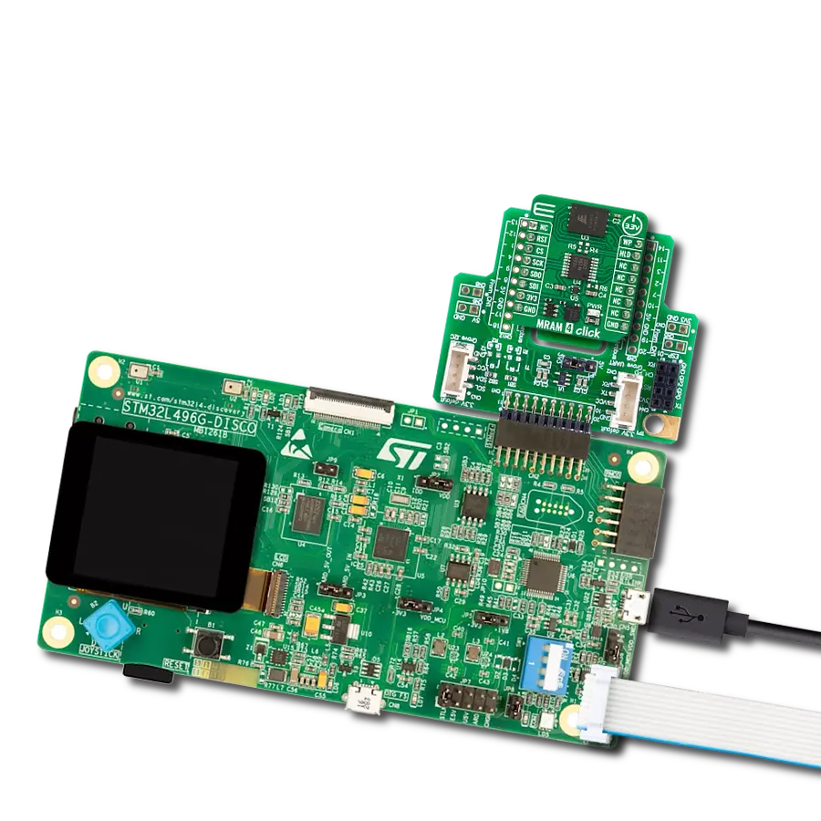
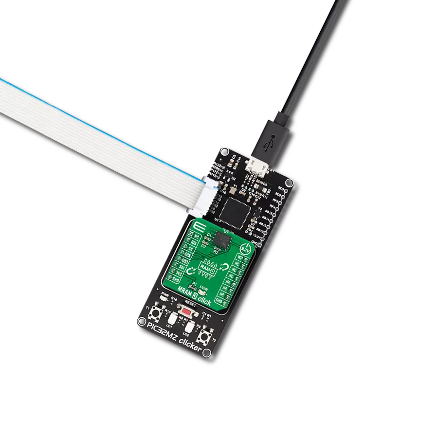
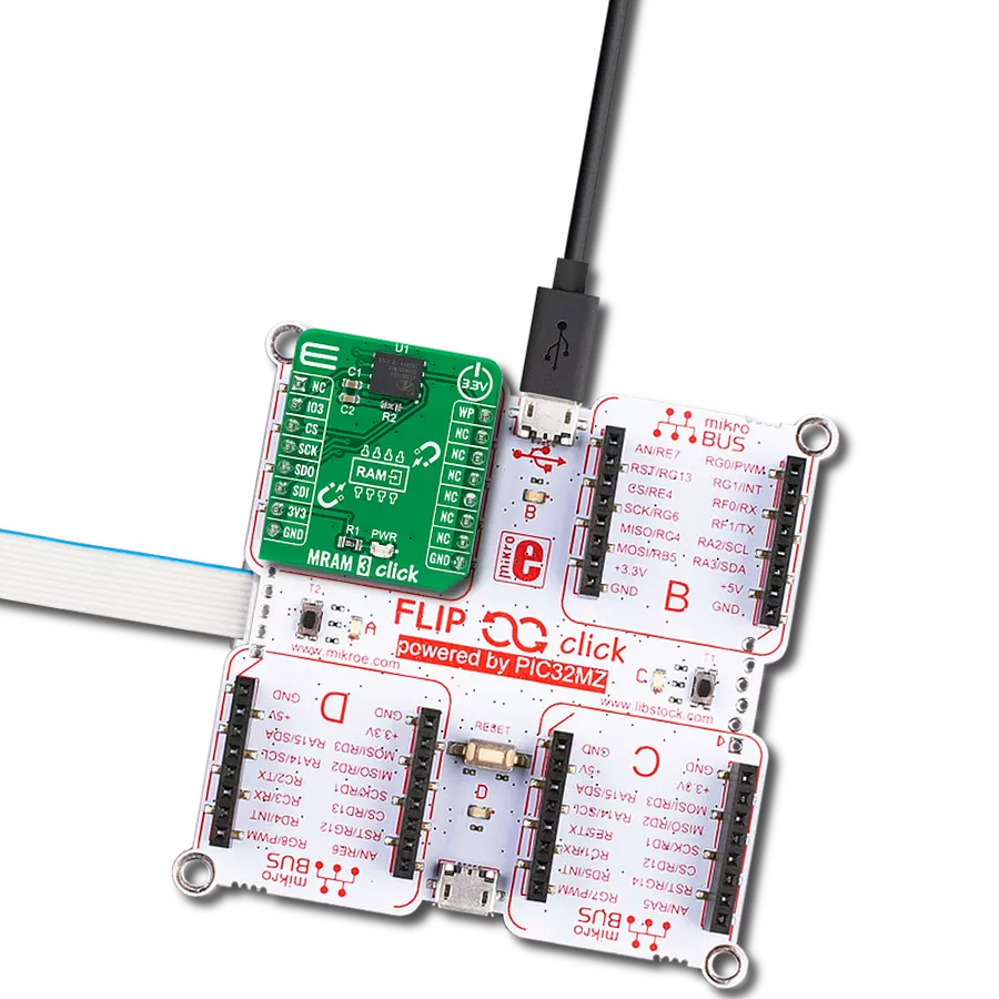
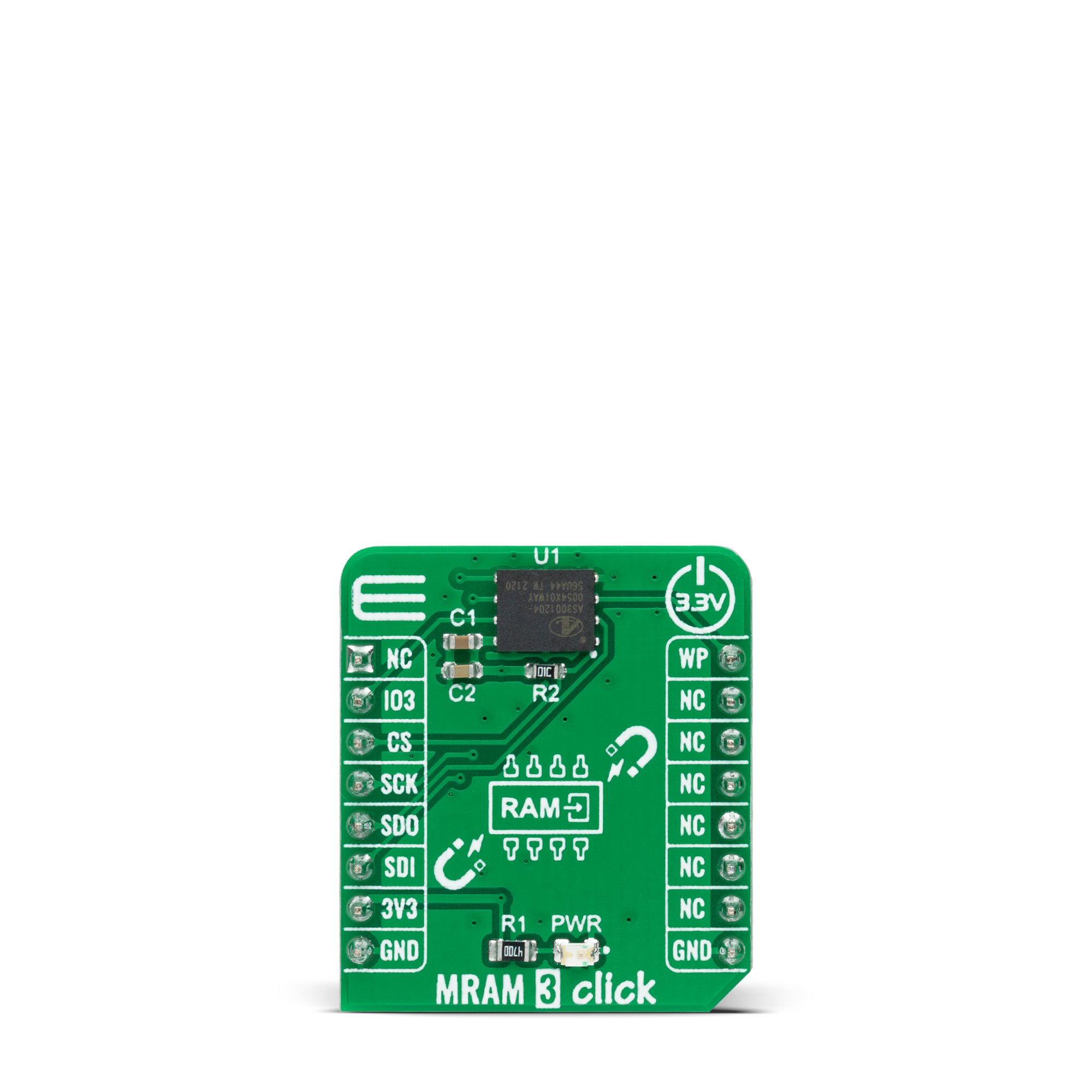
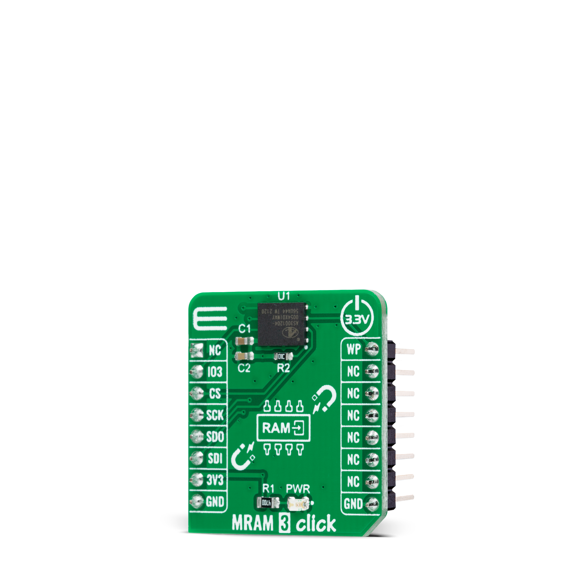
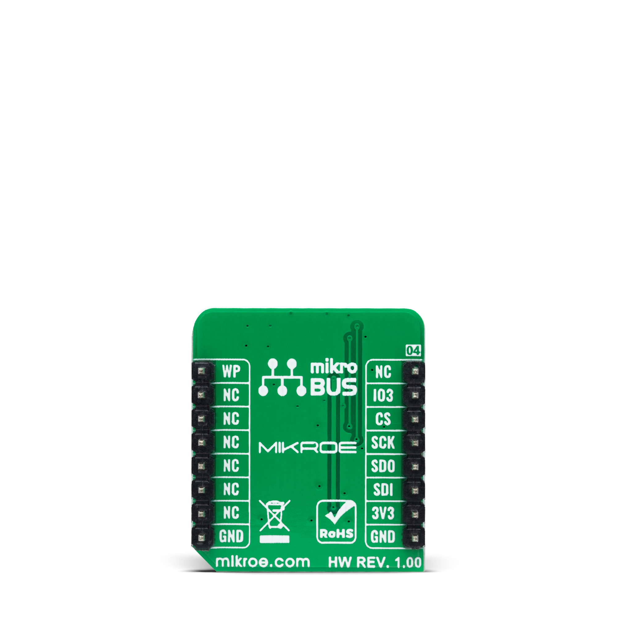
MRAM 3 Click
Dev. board
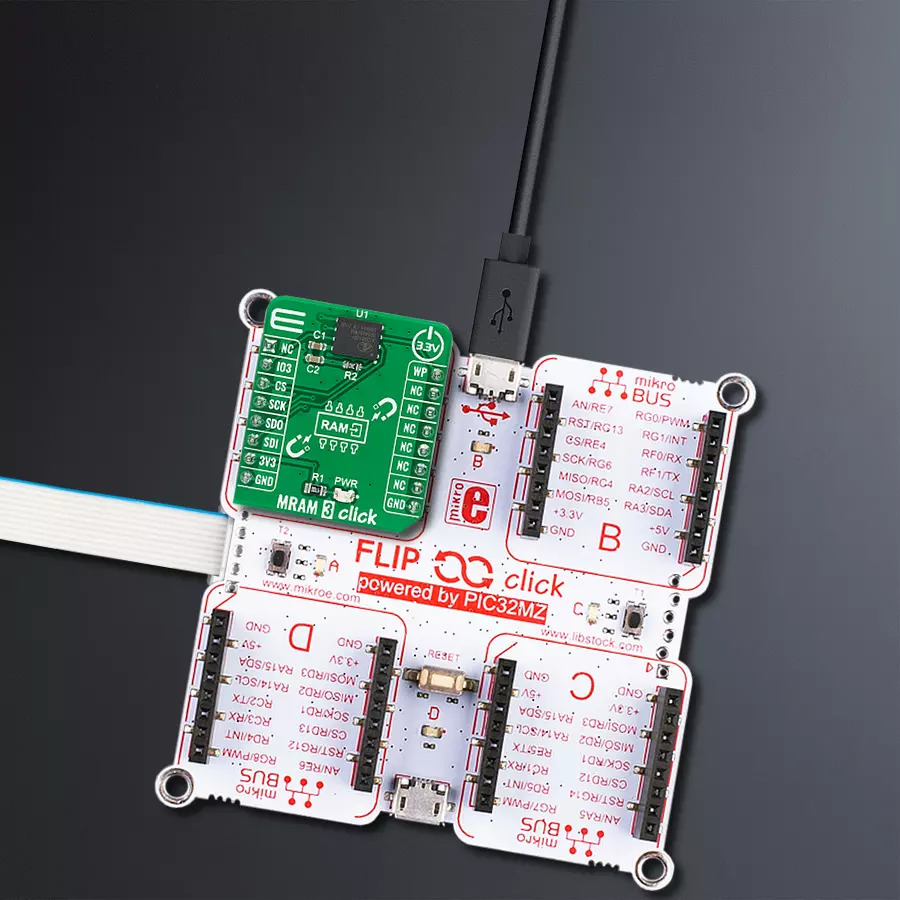
Flip&Click PIC32MZ
Compiler
NECTO Studio
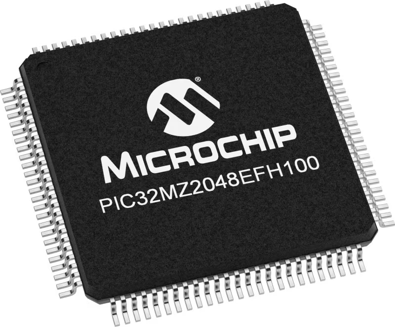
MCU
PIC32MZ2048EFH100
Fast and non-volatile magneto-resistive random-access memory
A
A
Hardware Overview
How does it work?
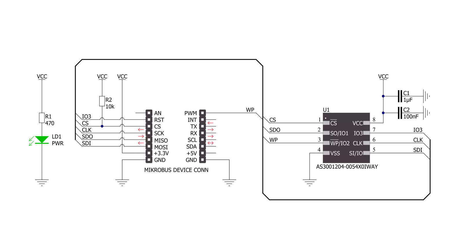
MRAM 3 Click is based on the AS3001204, a 1Mb MRAM memory with an SPI interface and Write Protection feature from Avalanche Technology. The AS3001204 is organized as 128K words of 8 bits each and benefits from 1.000.000 years of data retention combining their unprecedented data storage with excellent energy efficiency. It is highly reliable, lasting 1014 full-memory read/write/erase cycles, which makes this Click board™ suitable for high-reliability applications as a non-volatile storage media or temporary RAM expansion for storing data in any embedded application. The AS3001204 is an accurate random-access memory that allows both reads and writes to occur randomly. It offers low latency, low power, and scalable non-volatile memory
technology. The MRAM technology is analog to Flash technology with SRAM-compatible read/write timings (Persistent SRAM, P-SRAM), where data is always non-volatile. MRAM 3 Click communicates with MCU using the SPI serial interface that supports the Dual/Quad SPI and the two most common modes, SPI Mode 0 and 3, with a maximum SPI frequency of 108MHz. Alongside an SPI-compatible bus interface, the AS3001204 also features an eXecute-In-Place (XIP) functionality which allows completing a series of reading and writing instructions without having to individually load the read or write command for each instruction and hardware/software-based data protection mechanisms. Hardware Write Protection function, labeled and routed to the WP pin
of the mikroBUS™ socket, allows the user to freeze the entire memory area, thus protecting it from writing instructions. The IO3 pin of the mikroBUS™ socket is bidirectional I/O that transfers data into and out of the device in Dual and Quad SPI modes. This Click board™ can only be operated from a 3.3V logic voltage level. Therefore, the board must perform appropriate logic voltage conversion before using MCUs with different logic levels. However, the Click board™ comes equipped with a library containing functions and an example code that can be used as a reference for further development.
Features overview
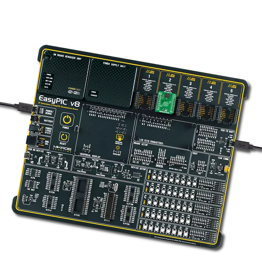
Development board
Flip&Click PIC32MZ is a compact development board designed as a complete solution that brings the flexibility of add-on Click boards™ to your favorite microcontroller, making it a perfect starter kit for implementing your ideas. It comes with an onboard 32-bit PIC32MZ microcontroller, the PIC32MZ2048EFH100 from Microchip, four mikroBUS™ sockets for Click board™ connectivity, two USB connectors, LED indicators, buttons, debugger/programmer connectors, and two headers compatible with Arduino-UNO pinout. Thanks to innovative manufacturing technology,
it allows you to build gadgets with unique functionalities and features quickly. Each part of the Flip&Click PIC32MZ development kit contains the components necessary for the most efficient operation of the same board. In addition, there is the possibility of choosing the Flip&Click PIC32MZ programming method, using the chipKIT bootloader (Arduino-style development environment) or our USB HID bootloader using mikroC, mikroBasic, and mikroPascal for PIC32. This kit includes a clean and regulated power supply block through the USB Type-C (USB-C) connector. All communication
methods that mikroBUS™ itself supports are on this board, including the well-established mikroBUS™ socket, user-configurable buttons, and LED indicators. Flip&Click PIC32MZ development kit allows you to create a new application in minutes. Natively supported by Mikroe software tools, it covers many aspects of prototyping thanks to a considerable number of different Click boards™ (over a thousand boards), the number of which is growing every day.

Microcontroller Overview
MCU Card / MCU
Architecture
PIC32
MCU Memory (KB)
2048
Silicon Vendor
Microchip
Pin count
100
RAM (Bytes)
524288
Used MCU Pins
mikroBUS™ mapper
Take a closer look
Click board™ Schematic
Step by step
Project assembly

Start by selecting your development board and Click board™. Begin with the Flip&Click PIC32MZ as your development board.


Software Support
Library Description
This library contains API for MRAM 3 Click driver.
Key functions:
mram3_memory_writeThis function writes a desired number of data bytes starting from the selected memory address.mram3_memory_readThis function reads a desired number of data bytes starting from the selected memory address.mram3_aug_memory_writeThis function writes a desired number of data bytes starting from the selected augmented memory address.
Open Source
Code example
The complete application code and a ready-to-use project are available through the NECTO Studio Package Manager for direct installation in the NECTO Studio. The application code can also be found on the MIKROE GitHub account.
/*!
 * @file main.c
 * @brief MRAM3 Click example
 *
 * # Description
 * This example demonstrates the use of MRAM 3 Click board by writing specified data to
 * the memory and reading it back.
 *
 * The demo application is composed of two sections :
 *
 * ## Application Init
 * Initializes the driver and performs the Click default configuration.
 *
 * ## Application Task
 * Writes a desired number of bytes to the memory and then verifies if it is written correctly
 * by reading from the same memory location and displaying the memory content on the USB UART.
 *
 * @author Stefan Filipovic
 *
 */

#include "board.h"
#include "log.h"
#include "mram3.h"

static mram3_t mram3;
static log_t logger;

#define DEMO_TEXT_MESSAGE_1         "MikroE"
#define DEMO_TEXT_MESSAGE_2         "MRAM 3 Click"
#define STARTING_ADDRESS            0x01234

void application_init ( void )
{
    log_cfg_t log_cfg;  /**< Logger config object. */
    mram3_cfg_t mram3_cfg;  /**< Click config object. */

    /**
     * Logger initialization.
     * Default baud rate: 115200
     * Default log level: LOG_LEVEL_DEBUG
     * @note If USB_UART_RX and USB_UART_TX
     * are defined as HAL_PIN_NC, you will
     * need to define them manually for log to work.
     * See @b LOG_MAP_USB_UART macro definition for detailed explanation.
     */
    LOG_MAP_USB_UART( log_cfg );
    log_init( &logger, &log_cfg );
    log_info( &logger, " Application Init " );

    // Click initialization.
    mram3_cfg_setup( &mram3_cfg );
    MRAM3_MAP_MIKROBUS( mram3_cfg, MIKROBUS_1 );
    if ( SPI_MASTER_ERROR == mram3_init( &mram3, &mram3_cfg ) )
    {
        log_error( &logger, " Communication init." );
        for ( ; ; );
    }

    if ( MRAM3_ERROR == mram3_default_cfg ( &mram3 ) )
    {
        log_error( &logger, " Default configuration." );
        for ( ; ; );
    }

    log_info( &logger, " Application Task " );
}

void application_task ( void )
{
    uint8_t data_buf[ 128 ] = { 0 };
    memcpy ( data_buf, DEMO_TEXT_MESSAGE_1, strlen ( DEMO_TEXT_MESSAGE_1 ) );
    if ( MRAM3_OK == mram3_memory_write ( &mram3, STARTING_ADDRESS,
                                          data_buf, sizeof ( data_buf ) ) )
    {
        log_printf ( &logger, "Data written to address 0x%.5LX: %s\r\n", ( uint32_t ) STARTING_ADDRESS,
                                                                                      data_buf );
    }
    memset ( data_buf, 0, sizeof ( data_buf ) );
    if ( MRAM3_OK == mram3_memory_read ( &mram3, STARTING_ADDRESS,
                                         data_buf, sizeof ( data_buf ) ) )
    {
        log_printf ( &logger, "Data read from address  0x%.5LX: %s\r\n", ( uint32_t ) STARTING_ADDRESS,
                                                                                      data_buf );
        Delay_ms ( 1000 );
        Delay_ms ( 1000 );
        Delay_ms ( 1000 );
    }
    memcpy ( data_buf, DEMO_TEXT_MESSAGE_2, strlen ( DEMO_TEXT_MESSAGE_2 ) );
    if ( MRAM3_OK == mram3_memory_write ( &mram3, STARTING_ADDRESS,
                                          data_buf, sizeof ( data_buf ) ) )
    {
        log_printf ( &logger, "Data written to address 0x%.5LX: %s\r\n", ( uint32_t ) STARTING_ADDRESS,
                                                                                      data_buf );
    }
    memset ( data_buf, 0, sizeof ( data_buf ) );
    if ( MRAM3_OK == mram3_memory_read ( &mram3, STARTING_ADDRESS,
                                         data_buf, sizeof ( data_buf ) ) )
    {
        log_printf ( &logger, "Data read from address  0x%.5LX: %s\r\n\n", ( uint32_t ) STARTING_ADDRESS,
                                                                                        data_buf );
        Delay_ms ( 1000 );
        Delay_ms ( 1000 );
        Delay_ms ( 1000 );
    }
}

int main ( void )
{
    /* Do not remove this line or clock might not be set correctly. */
    #ifdef PREINIT_SUPPORTED
    preinit();
    #endif

    application_init( );

    for ( ; ; )
    {
        application_task( );
    }

    return 0;
}

// ------------------------------------------------------------------------ END
Additional Support
Resources
Category:MRAM