Achieve data storage and access speeds previously thought impossible with the help of MR10Q010 and ATmega328P
Next-Gen memory marvel

Published Feb 14, 2024
Click board™
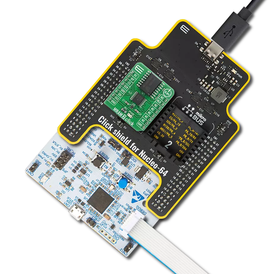
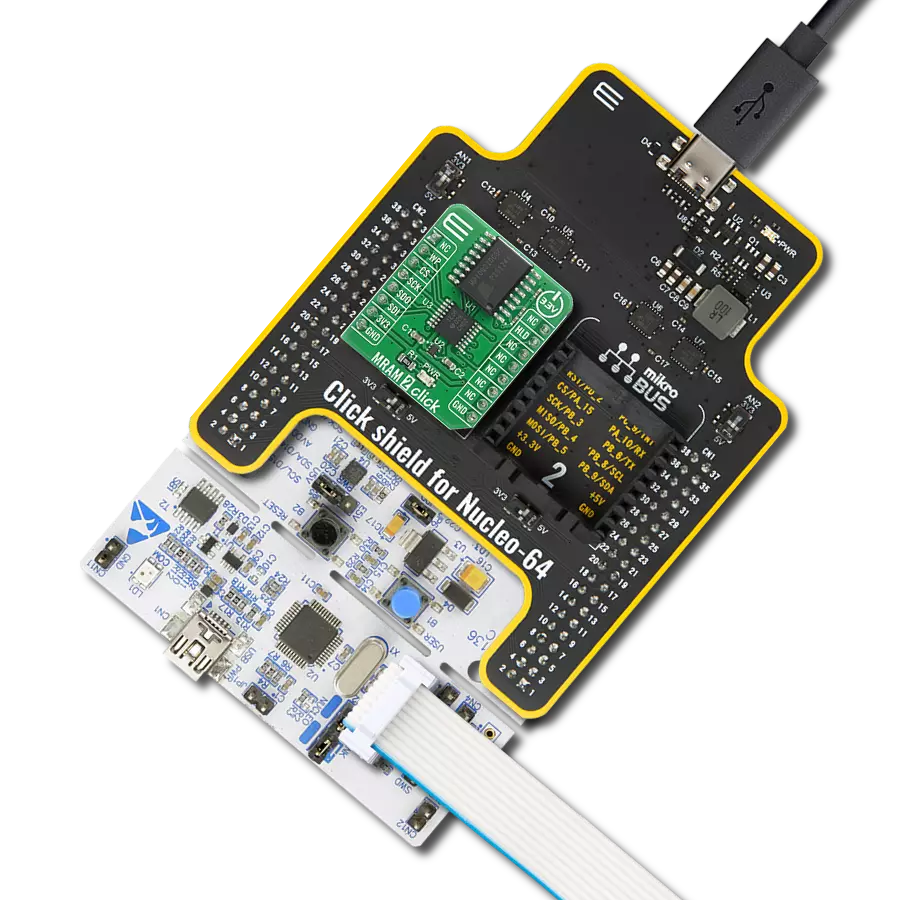
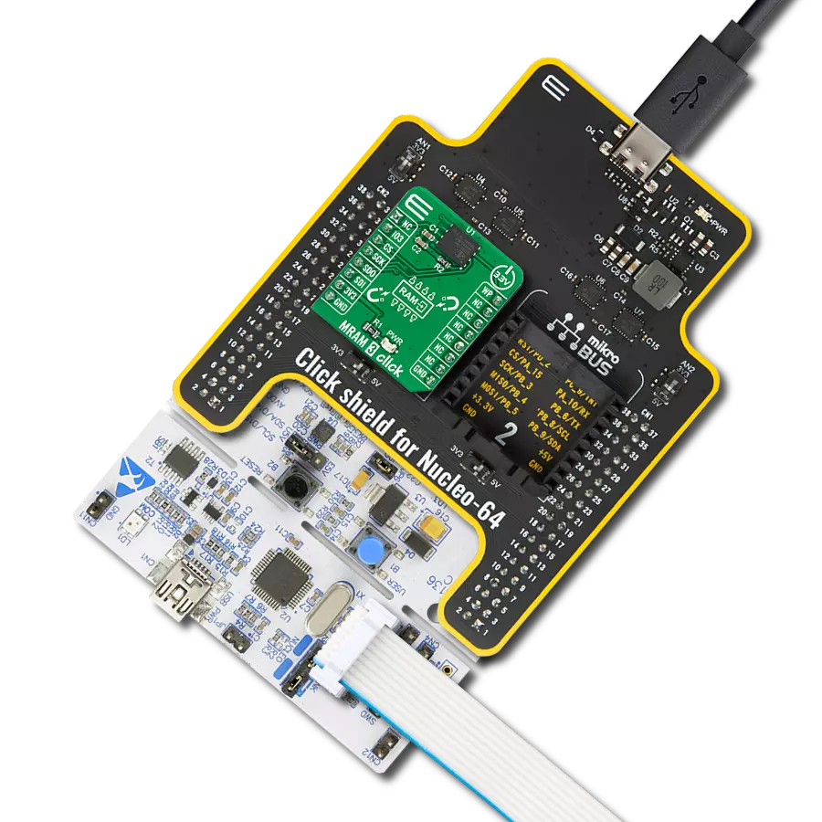
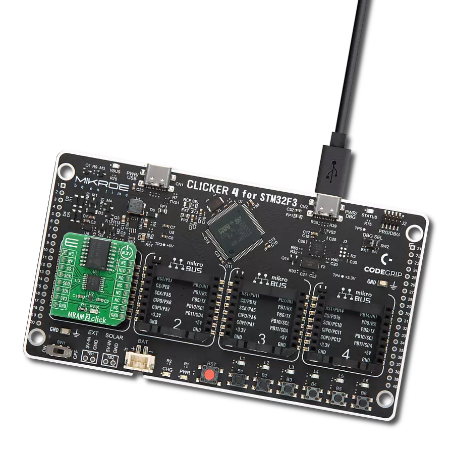
MRAM 2 Click
Dev. board
Arduino UNO Rev3
Compiler
NECTO Studio
MCU
ATmega328P
Significantly improve your solution by storing more data, enabling faster data access, and consuming less energy than existing electronic memory
A
A
Hardware Overview
How does it work?
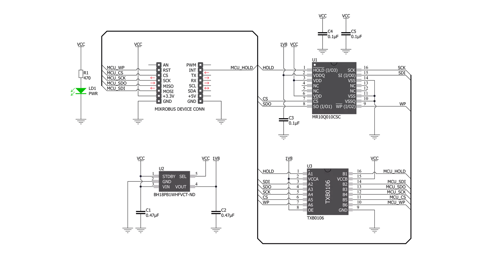
MRAM 2 Click is based on the MR10Q010, 1Mb Quad Output High-Speed Serial SPI MRAM memory solution from Everspin Technologies. The MR10Q010 is the ideal memory solution for applications that must quickly store and retrieve data and programs using a small number of pins, low power, and the space-saving 16-pin SOIC package. The four I/O’s in Quad SPI mode allow fast reads and writes, making it an attractive alternative to conventional parallel data bus interfaces in next-generation RAID controllers, server system logs, storage device buffers, and embedded system data and program memory. This Click board™ includes an LDO regulator BH18PB1WHFVCT from Rohm Semiconductor to provide the 1.8 V supply voltage. The LDO cuts power consumption by lowering its current
consumption to approximately 2μA when the application operates in the standby state. During normal-current operation, it will automatically switch to high-speed operating mode. The LDO regulator output provides a needed reference voltage for one side of the TXB0106, a 6-bit bidirectional level shifting and voltage translator with automatic direction sensing from Texas Instruments. The reference voltage for the other side of the level shifter is taken from the 3.3V pin from the mikroBUS™. The MRAM 2 Click communicates with MCU using the standard SPI serial interface that supports SPI Mode 0 and 3 and operates at clock rates up to 104 MHz. It also supports modes like Quad Peripheral Interface (QPI) and Quad SPI organized as 131.072 words of 8 bits. Both read and write operations can occur
randomly in memory without delay between writes. The MR10Q010 uses a Write Protect signal routed to the RST pin on the mikroBUS™ to prevent write operations to the Status Register, while the HOLD signal routed to the INT pin on the mikroBUS™ is used to interrupt a memory operation for another task. When HOLD is low, the current operation is suspended. This Click Board™ is designed to be operated only with a 3.3V logic level. A proper logic voltage level conversion should be performed before the Click board™ is used with MCUs with different logic levels. More information about the MR10Q010 can be found in the attached datasheet. Also, this Click board™ comes equipped with a library containing easy-to-use functions and an example code that can be used as a reference for further development.


Features overview
Development board
Arduino UNO is a versatile microcontroller board built around the ATmega328P chip. It offers extensive connectivity options for various projects, featuring 14 digital input/output pins, six of which are PWM-capable, along with six analog inputs. Its core components include a 16MHz ceramic resonator, a USB connection, a power jack, an
ICSP header, and a reset button, providing everything necessary to power and program the board. The Uno is ready to go, whether connected to a computer via USB or powered by an AC-to-DC adapter or battery. As the first USB Arduino board, it serves as the benchmark for the Arduino platform, with "Uno" symbolizing its status as the
first in a series. This name choice, meaning "one" in Italian, commemorates the launch of Arduino Software (IDE) 1.0. Initially introduced alongside version 1.0 of the Arduino Software (IDE), the Uno has since become the foundational model for subsequent Arduino releases, embodying the platform's evolution.

Microcontroller Overview
MCU Card / MCU

Architecture
AVR
MCU Memory (KB)
32
Silicon Vendor
Microchip
Pin count
28
RAM (Bytes)
2048
You complete me!
Accessories
Click Shield for Arduino UNO has two proprietary mikroBUS™ sockets, allowing all the Click board™ devices to be interfaced with the Arduino UNO board without effort. The Arduino Uno, a microcontroller board based on the ATmega328P, provides an affordable and flexible way for users to try out new concepts and build prototypes with the ATmega328P microcontroller from various combinations of performance, power consumption, and features. The Arduino Uno has 14 digital input/output pins (of which six can be used as PWM outputs), six analog inputs, a 16 MHz ceramic resonator (CSTCE16M0V53-R0), a USB connection, a power jack, an ICSP header, and reset button. Most of the ATmega328P microcontroller pins are brought to the IO pins on the left and right edge of the board, which are then connected to two existing mikroBUS™ sockets. This Click Shield also has several switches that perform functions such as selecting the logic levels of analog signals on mikroBUS™ sockets and selecting logic voltage levels of the mikroBUS™ sockets themselves. Besides, the user is offered the possibility of using any Click board™ with the help of existing bidirectional level-shifting voltage translators, regardless of whether the Click board™ operates at a 3.3V or 5V logic voltage level. Once you connect the Arduino UNO board with our Click Shield for Arduino UNO, you can access hundreds of Click boards™, working with 3.3V or 5V logic voltage levels.

Used MCU Pins
mikroBUS™ mapper
Take a closer look
Click board™ Schematic
Step by step
Project assembly

Start by selecting your development board and Click board™. Begin with the Arduino UNO Rev3 as your development board.


Track your results in real time
Application Output
1. Application Output - In Debug mode, the 'Application Output' window enables real-time data monitoring, offering direct insight into execution results. Ensure proper data display by configuring the environment correctly using the provided tutorial.

2. UART Terminal - Use the UART Terminal to monitor data transmission via a USB to UART converter, allowing direct communication between the Click board™ and your development system. Configure the baud rate and other serial settings according to your project's requirements to ensure proper functionality. For step-by-step setup instructions, refer to the provided tutorial.

3. Plot Output - The Plot feature offers a powerful way to visualize real-time sensor data, enabling trend analysis, debugging, and comparison of multiple data points. To set it up correctly, follow the provided tutorial, which includes a step-by-step example of using the Plot feature to display Click board™ readings. To use the Plot feature in your code, use the function: plot(*insert_graph_name*, variable_name);. This is a general format, and it is up to the user to replace 'insert_graph_name' with the actual graph name and 'variable_name' with the parameter to be displayed.

Software Support
Library Description
This library contains API for MRAM 2 Click driver.
Key functions:
mram2_wren- Write Enable functionmram2_read- Read Data Bytes functionmram2_write- Write Data Bytes function
Open Source
Code example
The complete application code and a ready-to-use project are available through the NECTO Studio Package Manager for direct installation in the NECTO Studio. The application code can also be found on the MIKROE GitHub account.
/*!
 * \file
 * \brief Mram2 Click example
 *
 * # Description
 * This example demonstrates the use of MRAM 2 Click board.
 *
 * The demo application is composed of two sections :
 *
 * ## Application Init
 * Initializes the driver, sets the write protect and disables the hold signal.
 *
 * ## Application Task
 * Writes "MikroE" into the first 6 memory locations, and then reads it back
 * and displays it to the USB UART approximately every 5 seconds.
 *
 * \author MikroE Team
 *
 */
// ------------------------------------------------------------------- INCLUDES

#include "board.h"
#include "log.h"
#include "mram2.h"

// ------------------------------------------------------------------ VARIABLES

static mram2_t mram2;
static log_t logger;

char val_in[ 7 ] = { 'M', 'i', 'k', 'r', 'o', 'E', 0 };
char val_out[ 7 ] = { 0 };

// ------------------------------------------------------ APPLICATION FUNCTIONS

void application_init ( void )
{
    log_cfg_t log_cfg;
    mram2_cfg_t cfg;

    /**
     * Logger initialization.
     * Default baud rate: 115200
     * Default log level: LOG_LEVEL_DEBUG
     * @note If USB_UART_RX and USB_UART_TX
     * are defined as HAL_PIN_NC, you will
     * need to define them manually for log to work.
     * See @b LOG_MAP_USB_UART macro definition for detailed explanation.
     */
    LOG_MAP_USB_UART( log_cfg );
    log_init( &logger, &log_cfg );
    log_info( &logger, "---- Application Init ----" );

    //  Click initialization.

    mram2_cfg_setup( &cfg );
    MRAM2_MAP_MIKROBUS( cfg, MIKROBUS_1 );
    mram2_init( &mram2, &cfg );

    log_printf( &logger, "------------------- \r\n" );
    log_printf( &logger, "   MRAM 2 Click     \r\n" );
    log_printf( &logger, "------------------- \r\n" );
    mram2_write_protect( &mram2, MRAM2_WP_ENABLE );
    mram2_hold( &mram2, MRAM2_HLD_DISABLE );
    log_printf( &logger, "   Initialized      \r\n" );
    log_printf( &logger, "------------------- \r\n" );
    Delay_ms ( 100 );
}

void application_task ( void )
{
    mram2_wren( &mram2 );
    log_printf( &logger, "Write enabled!\r\n" );
    Delay_ms ( 100 );
    log_printf( &logger, "Writing \"%s\" to memory...\r\n", val_in );
    mram2_write( &mram2, 0x000000, &val_in[ 0 ], 6 );
    Delay_ms ( 100 );
    mram2_wrdi ( &mram2 );
    log_printf( &logger, "Write disabled!\r\n" );
    Delay_ms ( 100 );
    mram2_read ( &mram2, 0x000000, &val_out[ 0 ], 6 );
    log_printf( &logger, "Read data : %s\r\n", val_out );

    log_printf( &logger, "-------------------\r\n" );
    Delay_ms ( 1000 );
    Delay_ms ( 1000 );
    Delay_ms ( 1000 );
    Delay_ms ( 1000 );
    Delay_ms ( 1000 );
}

int main ( void )
{
    /* Do not remove this line or clock might not be set correctly. */
    #ifdef PREINIT_SUPPORTED
    preinit();
    #endif

    application_init( );

    for ( ; ; )
    {
        application_task( );
    }

    return 0;
}

// ------------------------------------------------------------------------ END
Additional Support
Resources
Category:MRAM