Achieve 16-bit analog signal conversion with MAX1302 and STM32G474RE
High-resolution, multi-channel ADC solution for precise analog signal conversion
Published Jul 10, 2025
Click board™
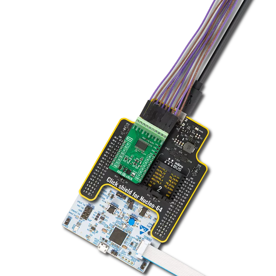
ADC 27 Click
Dev. board
Nucleo 64 with STM32G474RE MCU
Compiler
NECTO Studio
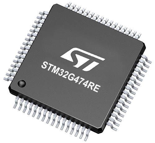
MCU
STM32G474RE
Experience high-resolution data acquisition with eight single-ended or four differential input channels
A
A
Hardware Overview
How does it work?
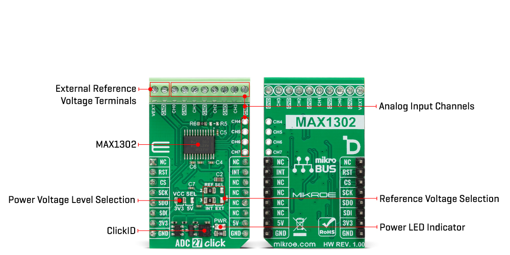
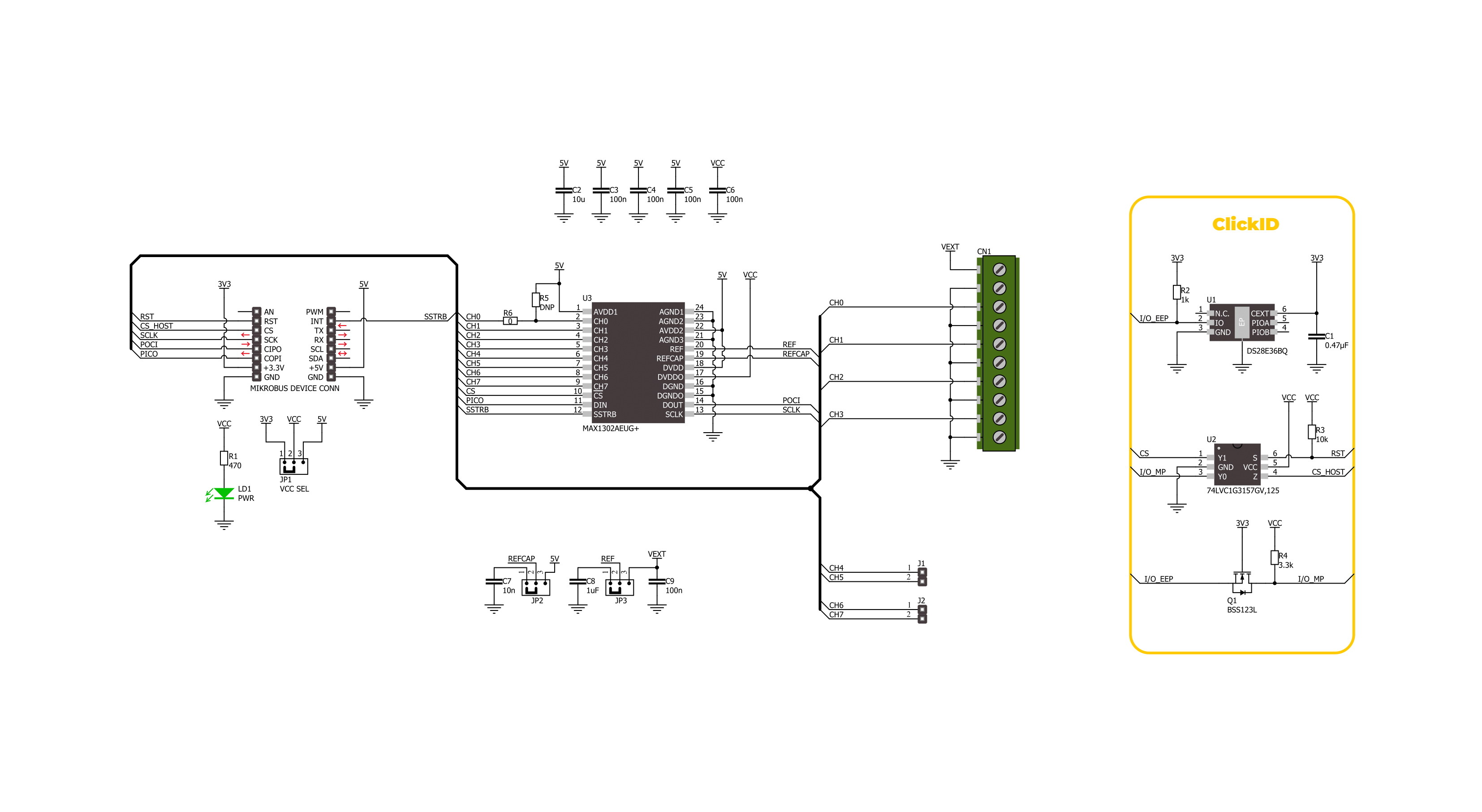
ADC 27 Click is based on the MAX1302, a multirange 16-bit successive-approximation ADC from Analog Devices that supports throughput rates of up to 115ksps and offers remarkable flexibility in analog signal sampling. It communicates with the host MCU via a high-speed SPI-compatible interface, ensuring integration into a wide range of embedded applications. The MAX1302 provides eight single-ended or four true differential analog input channels, each of which can be independently configured in software for various input voltage ranges. Specifically, the single-ended mode supports seven programmable ranges, including 0V to +VREF/2, -VREF/2 to 0V, 0V to +VREF, -VREF to 0V, ±VREF/4, ±VREF/2, and ±VREF, while the
differential mode supports three programmable ranges: ±VREF/2, ±VREF, and ±2×VREF. This enables highly adaptable signal conditioning depending on the application's accuracy and range requirements. The MAX1302 includes an internal precision +4.096V reference voltage, simplifying design. Yet it also allows the use of an external reference voltage between 3.800V and 4.136V for enhanced flexibility, which can be selected by setting the onboard REF SEL jumper to either INT for internal or EXT for external reference. Designed for demanding analog measurement tasks, ADC 27 Click is well-suited for use in industrial monitoring, control systems, data acquisition setups, avionics instrumentation, and robotics, providing robust
performance in environments where accuracy and configurability are essential. In addition to the standard SPI communication pins (SDO, SDI, SCK, and CS), ADC 27 Click also uses an INT pin, which serves as a data-ready indicator. This interrupt pin becomes active when a new conversion result is available, signaling the host MCU that data is ready to be read. This Click board™ can operate with either 3.3V or 5V logic voltage levels selected via the VCC SEL jumper. This way, both 3.3V and 5V capable MCUs can use the communication lines properly. Also, this Click board™ comes equipped with a library containing easy-to-use functions and an example code that can be used as a reference for further development.
Features overview
Development board
Nucleo-64 with STM32G474R MCU offers a cost-effective and adaptable platform for developers to explore new ideas and prototype their designs. This board harnesses the versatility of the STM32 microcontroller, enabling users to select the optimal balance of performance and power consumption for their projects. It accommodates the STM32 microcontroller in the LQFP64 package and includes essential components such as a user LED, which doubles as an ARDUINO® signal, alongside user and reset push-buttons, and a 32.768kHz crystal oscillator for precise timing operations. Designed with expansion and flexibility in mind, the Nucleo-64 board features an ARDUINO® Uno V3 expansion connector and ST morpho extension pin
headers, granting complete access to the STM32's I/Os for comprehensive project integration. Power supply options are adaptable, supporting ST-LINK USB VBUS or external power sources, ensuring adaptability in various development environments. The board also has an on-board ST-LINK debugger/programmer with USB re-enumeration capability, simplifying the programming and debugging process. Moreover, the board is designed to simplify advanced development with its external SMPS for efficient Vcore logic supply, support for USB Device full speed or USB SNK/UFP full speed, and built-in cryptographic features, enhancing both the power efficiency and security of projects. Additional connectivity is
provided through dedicated connectors for external SMPS experimentation, a USB connector for the ST-LINK, and a MIPI® debug connector, expanding the possibilities for hardware interfacing and experimentation. Developers will find extensive support through comprehensive free software libraries and examples, courtesy of the STM32Cube MCU Package. This, combined with compatibility with a wide array of Integrated Development Environments (IDEs), including IAR Embedded Workbench®, MDK-ARM, and STM32CubeIDE, ensures a smooth and efficient development experience, allowing users to fully leverage the capabilities of the Nucleo-64 board in their projects.

Microcontroller Overview
MCU Card / MCU
Architecture
ARM Cortex-M4
MCU Memory (KB)
512
Silicon Vendor
STMicroelectronics
Pin count
64
RAM (Bytes)
128k
You complete me!
Accessories
Click Shield for Nucleo-64 comes equipped with two proprietary mikroBUS™ sockets, allowing all the Click board™ devices to be interfaced with the STM32 Nucleo-64 board with no effort. This way, Mikroe allows its users to add any functionality from our ever-growing range of Click boards™, such as WiFi, GSM, GPS, Bluetooth, ZigBee, environmental sensors, LEDs, speech recognition, motor control, movement sensors, and many more. More than 1537 Click boards™, which can be stacked and integrated, are at your disposal. The STM32 Nucleo-64 boards are based on the microcontrollers in 64-pin packages, a 32-bit MCU with an ARM Cortex M4 processor operating at 84MHz, 512Kb Flash, and 96KB SRAM, divided into two regions where the top section represents the ST-Link/V2 debugger and programmer while the bottom section of the board is an actual development board. These boards are controlled and powered conveniently through a USB connection to program and efficiently debug the Nucleo-64 board out of the box, with an additional USB cable connected to the USB mini port on the board. Most of the STM32 microcontroller pins are brought to the IO pins on the left and right edge of the board, which are then connected to two existing mikroBUS™ sockets. This Click Shield also has several switches that perform functions such as selecting the logic levels of analog signals on mikroBUS™ sockets and selecting logic voltage levels of the mikroBUS™ sockets themselves. Besides, the user is offered the possibility of using any Click board™ with the help of existing bidirectional level-shifting voltage translators, regardless of whether the Click board™ operates at a 3.3V or 5V logic voltage level. Once you connect the STM32 Nucleo-64 board with our Click Shield for Nucleo-64, you can access hundreds of Click boards™, working with 3.3V or 5V logic voltage levels.

Used MCU Pins
mikroBUS™ mapper
Take a closer look
Click board™ Schematic
Step by step
Project assembly
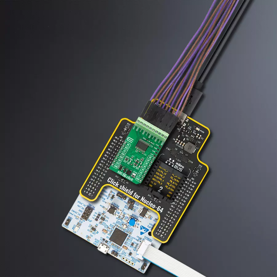
Start by selecting your development board and Click board™. Begin with the Nucleo 64 with STM32G474RE MCU as your development board.


Software Support
Library Description
ADC 27 Click demo application is developed using the NECTO Studio, ensuring compatibility with mikroSDK's open-source libraries and tools. Designed for plug-and-play implementation and testing, the demo is fully compatible with all development, starter, and mikromedia boards featuring a mikroBUS™ socket.
Example Description
This example demonstrates the use of the ADC 27 Click board by reading voltages from multiple analog input channels configured in both single-ended and differential modes. The measured voltage values are displayed via UART.
Key functions:
adc27_cfg_setup- This function initializes Click configuration structure to initial values.adc27_init- This function initializes all necessary pins and peripherals used for this Click board.adc27_default_cfg- This function executes a default configuration of ADC 27 Click board.adc27_set_config- This function sets the configuration for the selected channel of the ADC 27 Click board.adc27_read_raw_data- This function reads raw ADC data from the selected channel.adc27_read_voltage- This function reads the ADC value from the selected channel and converts it to a voltage level using the configured range.
Application Init
Initializes the logger and the ADC 27 Click driver, and performs the default configuration.
Application Task
Reads and logs voltage values from channels CH0-CH3 (single-ended) and CH4/CH5, CH6/CH7 (differential).
Open Source
Code example
The complete application code and a ready-to-use project are available through the NECTO Studio Package Manager for direct installation in the NECTO Studio. The application code can also be found on the MIKROE GitHub account.
/*!
 * @file main.c
 * @brief ADC 27 Click example
 *
 * # Description
 * This example demonstrates the use of the ADC 27 Click board by reading voltages
 * from multiple analog input channels configured in both single-ended and differential modes.
 * The measured voltage values are displayed via UART.
 *
 * The demo application is composed of two sections:
 *
 * ## Application Init
 * Initializes the logger and the ADC 27 Click driver, and performs the default configuration.
 *
 * ## Application Task
 * Reads and logs voltage values from channels CH0-CH3 (single-ended) and CH4/CH5, CH6/CH7 (differential).
 *
 * @note
 * CH0 and CH1 operate with respect to ground and VREF, while CH2 and CH3 provide bipolar inputs.
 * Channels CH4/CH5 and CH6/CH7 are differential input pairs. Measurements are taken every second.
 *
 * @author Stefan Filipovic
 *
 */

#include "board.h"
#include "log.h"
#include "adc27.h"

static adc27_t adc27;
static log_t logger;

void application_init ( void )
{
    log_cfg_t log_cfg;  /**< Logger config object. */
    adc27_cfg_t adc27_cfg;  /**< Click config object. */

    /**
     * Logger initialization.
     * Default baud rate: 115200
     * Default log level: LOG_LEVEL_DEBUG
     * @note If USB_UART_RX and USB_UART_TX
     * are defined as HAL_PIN_NC, you will
     * need to define them manually for log to work.
     * See @b LOG_MAP_USB_UART macro definition for detailed explanation.
     */
    LOG_MAP_USB_UART( log_cfg );
    log_init( &logger, &log_cfg );
    log_info( &logger, " Application Init " );

    // Click initialization.
    adc27_cfg_setup( &adc27_cfg );
    ADC27_MAP_MIKROBUS( adc27_cfg, MIKROBUS_1 );
    if ( SPI_MASTER_ERROR == adc27_init( &adc27, &adc27_cfg ) )
    {
        log_error( &logger, " Communication init." );
        for ( ; ; );
    }

    if ( ADC27_ERROR == adc27_default_cfg ( &adc27 ) )
    {
        log_error( &logger, " Default configuration." );
        for ( ; ; );
    }

    log_info( &logger, " Application Task " );
}

void application_task ( void )
{
    float voltage = 0;
    if ( ADC27_OK == adc27_read_voltage ( &adc27, ADC27_CONFIG_CH_SGL_0, &voltage ) )
    {
        log_printf ( &logger, " CH0: %.3f V (gnd,vref/2)\r\n", voltage );
    }
    if ( ADC27_OK == adc27_read_voltage ( &adc27, ADC27_CONFIG_CH_SGL_1, &voltage ) )
    {
        log_printf ( &logger, " CH1: %.3f V (gnd,vref)\r\n", voltage );
    }
    if ( ADC27_OK == adc27_read_voltage ( &adc27, ADC27_CONFIG_CH_SGL_2, &voltage ) )
    {
        log_printf ( &logger, " CH2: %.3f V (-vref/4,vref/4)\r\n", voltage );
    }
    if ( ADC27_OK == adc27_read_voltage ( &adc27, ADC27_CONFIG_CH_SGL_3, &voltage ) )
    {
        log_printf ( &logger, " CH3: %.3f V (-vref/2,vref/2)\r\n", voltage );
    }
    if ( ADC27_OK == adc27_read_voltage ( &adc27, ADC27_CONFIG_CH_DIF_45, &voltage ) )
    {
        log_printf ( &logger, " CH4+/CH5-: %.3f V (-vref,vref)\r\n", voltage );
    }
    if ( ADC27_OK == adc27_read_voltage ( &adc27, ADC27_CONFIG_CH_DIF_67, &voltage ) )
    {
        log_printf ( &logger, " CH6+/CH7-: %.3f V (-2xvref,2xvref)\r\n\n", voltage );
    }
    Delay_ms ( 1000 );
}

int main ( void )
{
    /* Do not remove this line or clock might not be set correctly. */
    #ifdef PREINIT_SUPPORTED
    preinit();
    #endif

    application_init( );

    for ( ; ; )
    {
        application_task( );
    }

    return 0;
}

// ------------------------------------------------------------------------ END
Additional Support
Resources
Category:ADC


