Achieve real-time monitoring and control in automotive and industrial settings with ATA663211 and STM32L496AG
The future of low-speed data communication with LIN transceivers
Published Jul 22, 2025
Click board™
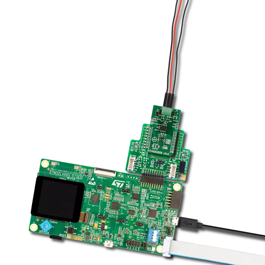
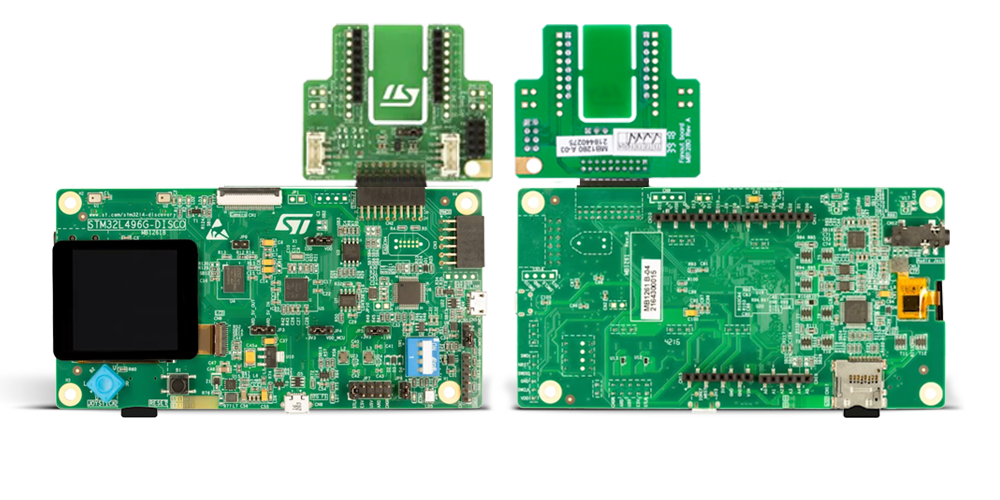
ATA663211 Click
Dev. board
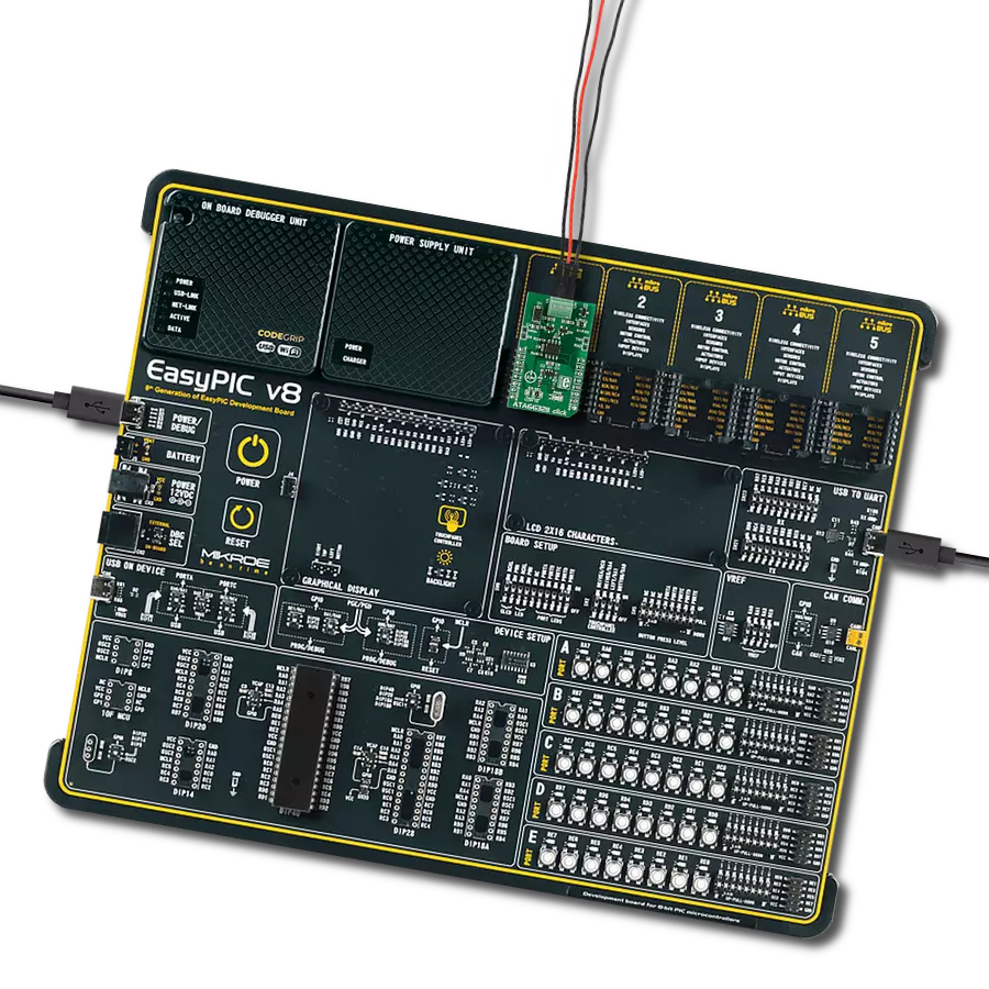
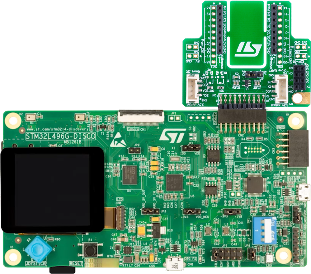
Discovery kit with STM32L496AG MCU
Compiler
NECTO Studio
MCU
STM32L496AG
Our LIN transceiver empowers vehicles and industrial systems to efficiently exchange critical data at low speeds, ensuring seamless communication
A
A
Hardware Overview
How does it work?
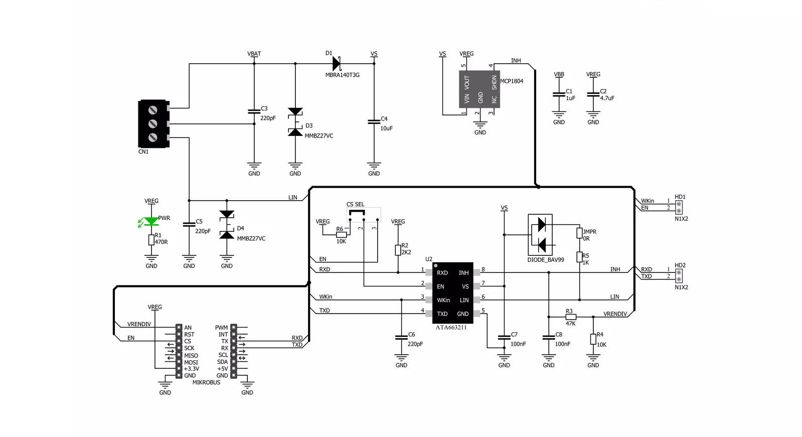
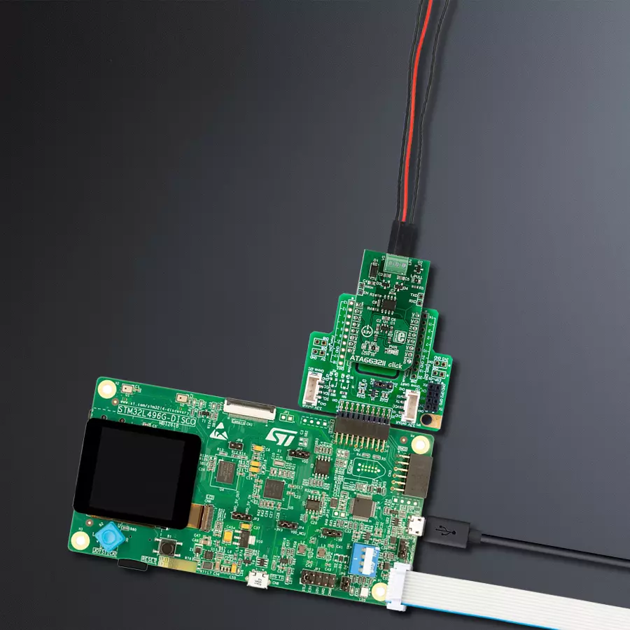
ATA663211 Click is based on the ATA663211, a LIN transceiver from Microchip. It features several protection functionalities, such as over-temperature, short-circuit protection vs. GND and battery, advanced EMC and ESD, and more. The integrated 3.3V onboard LDO voltage regulator is the MCP1804, an LDO regulator with shutdown from Microchip. The combination of a voltage regulator and a bus transceiver makes it possible to develop simple but powerful slave nodes in LIN bus systems. This way, ATA663211 Click can be used as a standalone LIN transceiver without being connected to a mikroBUS™ socket. An onboard LDO (low-dropout regulator) lets it supply power through the VS line screw terminal. This regulated voltage is also available on the +3.3V rail of the mikroBUS™ socket to power up the 3.3V attached host MCU. There are several operating modes for the ATA663211 Click. In Normal mode, the LIN interface is transmitting and receiving. In Sleep mode, the transmission path is disabled, and the LIN transceiver is in low-power mode. The Failsafe mode is automatically switched at system power-up or after a wake-up event. The LIN transceiver
is switched off in this mode, and the inhibit output pin is switched on. For the typical application as a Master node, the ATA663211 requires the LBUS line of the chip to be connected to the VBB of the LIN BUS, achievable via a populated L-PULL jumper. This jumper can be removed in other scenarios, such as the LIN Slave node. The ATA663211 communicates with the MCU using the UART RX and TX signals. Besides communication, these pins also serve to signal the failsafe condition. The undervoltage on the LIN connector can cause the failsafe condition: less than 3.9V will cause the undervoltage condition, signaled by the LOW logic state on the RX pin and the HIGH logic state on the TX pin. A LIN wake-up event from either silent or sleep mode is signaled by the LOW logic state on both the RX and TX pins. This event is received via the LIN bus and is used to switch the ATA663211 click to an active state. On the other hand, Low on TX and HIGH on RX will signal the local wake-up. RX and TX signals are also routed to the header on the edge of the Click board™ so they can be used independently of the mikroBUS™ socket. The inhibit output pin of the LIN transceiver is used
to control the Shutdown input of the MCP1804 LDO; thus, the supply pin of the LIN transceiver itself, as the LDO, supplies the LIN transceiver supply pin with LIN operating voltage. The voltages on this line can be monitored over the INH pin of the mikroBUS™ socket via the resistor divider. To enable the LIN transceiver, there is an EN SEL jumper set to the HI position by default, thus enabling the transceiver. Setting it to the LOW position allows you to control the enable function over the EN pin of the mikroBUS™ socket. In addition, this same pin is routed to the second pair of headers to enable the LIN transceiver externally. The other pin on this header is WKin, a high-voltage input for waking up the device. This Click board™ can be operated only with a 3.3V logic voltage level. The board must perform appropriate logic voltage level conversion before using MCUs with different logic levels. However, the Click board™ comes equipped with a library containing functions and an example code that can be used as a reference for further development.

Features overview
Development board
The 32L496GDISCOVERY Discovery kit serves as a comprehensive demonstration and development platform for the STM32L496AG microcontroller, featuring an Arm® Cortex®-M4 core. Designed for applications that demand a balance of high performance, advanced graphics, and ultra-low power consumption, this kit enables seamless prototyping for a wide range of embedded solutions. With its innovative energy-efficient
architecture, the STM32L496AG integrates extended RAM and the Chrom-ART Accelerator, enhancing graphics performance while maintaining low power consumption. This makes the kit particularly well-suited for applications involving audio processing, graphical user interfaces, and real-time data acquisition, where energy efficiency is a key requirement. For ease of development, the board includes an onboard ST-LINK/V2-1
debugger/programmer, providing a seamless out-of-the-box experience for loading, debugging, and testing applications without requiring additional hardware. The combination of low power features, enhanced memory capabilities, and built-in debugging tools makes the 32L496GDISCOVERY kit an ideal choice for prototyping advanced embedded systems with state-of-the-art energy efficiency.
Microcontroller Overview
MCU Card / MCU
Architecture
ARM Cortex-M4
MCU Memory (KB)
1024
Silicon Vendor
STMicroelectronics
Pin count
169
RAM (Bytes)
327680
Used MCU Pins
mikroBUS™ mapper
Take a closer look
Click board™ Schematic
Step by step
Project assembly
Start by selecting your development board and Click board™. Begin with the Discovery kit with STM32L496AG MCU as your development board.


Track your results in real time
Application Output
1. Application Output - In Debug mode, the 'Application Output' window enables real-time data monitoring, offering direct insight into execution results. Ensure proper data display by configuring the environment correctly using the provided tutorial.

2. UART Terminal - Use the UART Terminal to monitor data transmission via a USB to UART converter, allowing direct communication between the Click board™ and your development system. Configure the baud rate and other serial settings according to your project's requirements to ensure proper functionality. For step-by-step setup instructions, refer to the provided tutorial.

3. Plot Output - The Plot feature offers a powerful way to visualize real-time sensor data, enabling trend analysis, debugging, and comparison of multiple data points. To set it up correctly, follow the provided tutorial, which includes a step-by-step example of using the Plot feature to display Click board™ readings. To use the Plot feature in your code, use the function: plot(*insert_graph_name*, variable_name);. This is a general format, and it is up to the user to replace 'insert_graph_name' with the actual graph name and 'variable_name' with the parameter to be displayed.

Software Support
Library Description
This library contains API for ATA663211 Click driver.
Key functions:
ata663211_generic_write- Generic write functionata663211_generic_read- Generic read function.
Open Source
Code example
The complete application code and a ready-to-use project are available through the NECTO Studio Package Manager for direct installation in the NECTO Studio. The application code can also be found on the MIKROE GitHub account.
/*!
 * \file
 * \brief Ata663211 Click example
 *
 * # Description
 * This example demonstrates the use of an ATA663211 Click board by showing
 * the communication between the two Click boards.
 *
 * The demo application is composed of two sections :
 *
 * ## Application Init
 * Initalizes device and makes an initial log.
 *
 * ## Application Task
 * Depending on the selected application mode, it reads all the received data or
 * sends the desired text message with the message counter once per second.
 *
 * \author MikroE Team
 *
 */
// ------------------------------------------------------------------- INCLUDES

#include "board.h"
#include "log.h"
#include "ata663211.h"

// ------------------------------------------------------------------ VARIABLES

// Comment out the line below in order to switch the application mode to receiver
#define DEMO_APP_TRANSMITTER

// Text message to send in the transmitter application mode
#define DEMO_TEXT_MESSAGE           "MIKROE - ATA663211 Click board\r\n\0"

static ata663211_t ata663211;
static log_t logger;

// ------------------------------------------------------ APPLICATION FUNCTIONS

void application_init ( void )
{
    log_cfg_t log_cfg;
    ata663211_cfg_t cfg;

    /**
     * Logger initialization.
     * Default baud rate: 115200
     * Default log level: LOG_LEVEL_DEBUG
     * @note If USB_UART_RX and USB_UART_TX
     * are defined as HAL_PIN_NC, you will
     * need to define them manually for log to work.
     * See @b LOG_MAP_USB_UART macro definition for detailed explanation.
     */
    LOG_MAP_USB_UART( log_cfg );
    log_init( &logger, &log_cfg );
    log_info( &logger, "---- Application Init ----" );

    //  Click initialization.
    ata663211_cfg_setup( &cfg );
    ATA663211_MAP_MIKROBUS( cfg, MIKROBUS_1 );
    ata663211_init( &ata663211, &cfg );
#ifdef DEMO_APP_TRANSMITTER
    log_printf( &logger, " Application Mode: Transmitter\r\n" );
#else
    log_printf( &logger, " Application Mode: Receiver\r\n" );
#endif
}

void application_task ( void )
{
#ifdef DEMO_APP_TRANSMITTER
    ata663211_generic_write( &ata663211, DEMO_TEXT_MESSAGE, strlen( DEMO_TEXT_MESSAGE ) );
    log_printf( &logger, "%s", ( char * ) DEMO_TEXT_MESSAGE );
    Delay_ms ( 1000 );
#else
    uint8_t rx_byte = 0;
    if ( 1 == ata663211_generic_read( &ata663211, &rx_byte, 1 ) )
    {
       log_printf( &logger, "%c", rx_byte );
    }
#endif
}

int main ( void )
{
    /* Do not remove this line or clock might not be set correctly. */
    #ifdef PREINIT_SUPPORTED
    preinit();
    #endif

    application_init( );

    for ( ; ; )
    {
        application_task( );
    }

    return 0;
}


// ------------------------------------------------------------------------ END
Additional Support
Resources
Category:LIN