Achieve incredible success in analog multiplexing with CD74HC4067 and TM4C1294NCPDT
The ultimate analog switching solution

Published Sep 23, 2023
Click board™
Analog MUX Click
Dev. board
UNI-DS v8
Compiler
NECTO Studio
MCU
TM4C1294NCPDT
Achieve precise control over analog signals in complex systems with our 16-channel input switching solution optimized for high-performance applications in various industries
A
A
Hardware Overview
How does it work?
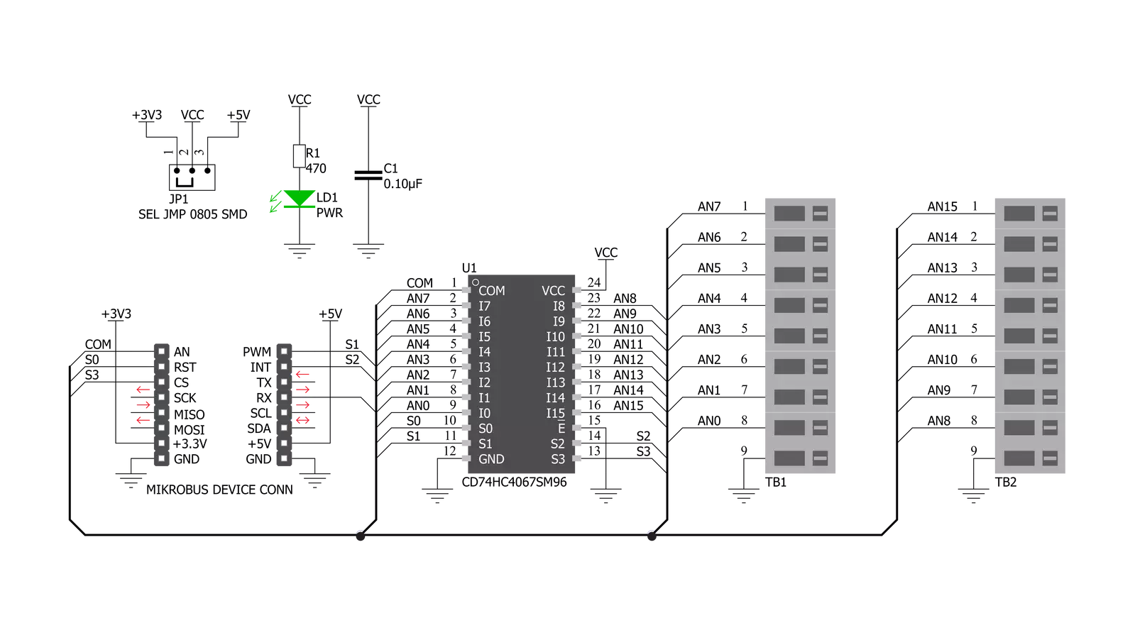
Analog MUX Click is based on the CD74HC4067, a high-speed CMOS logic 16-channel analog multiplexer/demultiplexer from Texas Instruments. It supports 3.3V and 5V power supplies, as well as rail-to-rail operation, allowing it to be used in various applications. Four control pins switch one of sixteen inputs to a single output. Control pins labeled as S0, S1, S2, and S3 are routed to the mikroBUS™ and can be operated by both 3.3V and 5V MCUs. These pins are routed to the RST, PWM, INT, and CS pins of the mikroBUS™, respectively, while the common output pin from the multiplexer is routed to the AN pin on the mikroBUS™. The CD74HC4067 IC is digitally controlled analog switch that utilize silicon-gate CMOS technology to achieve operating speeds similar to LSTTL, with the low power
consumption of standard CMOS integrated circuits. The mentioned analog multiplexer/demultiplexer control analog voltages that may vary across the voltage supply range. The ultra-low leakage current ensures that there is no signal interference from the inputs that are not selected by the S0, S1, S2, and S3 pins. A low crosstalk also ensures that the signal on one channel remains clean of interferences caused by other channels. To prevent any two inputs to be switched at the output at the same time, a break-before-make switching action is utilized. This ensures a reliable operation of the IC and the Click board™ itself. Analog MUX click is bidirectional switch as well, thus allowing any analog input to be used as an output and vice-versa. The switches have low “on” resistance and low “off” leakages.
All of the input channels can be easily connected to the two 9 pole spring action block terminals, without having to use any additional tools, such as screwdrivers. More information about the CD74HC4067 can be found in the attached datasheet. However, the Click board™ comes equipped with a library that contains easy to use functions and a usage example that may be used as a reference for the development. This Click board™ can operate with either 3.3V or 5V logic voltage levels selected via the VCC SEL jumper. This way, both 3.3V and 5V capable MCUs can use the communication lines properly. Also, this Click board™ comes equipped with a library containing easy-to-use functions and an example code that can be used as a reference for further development.


Features overview
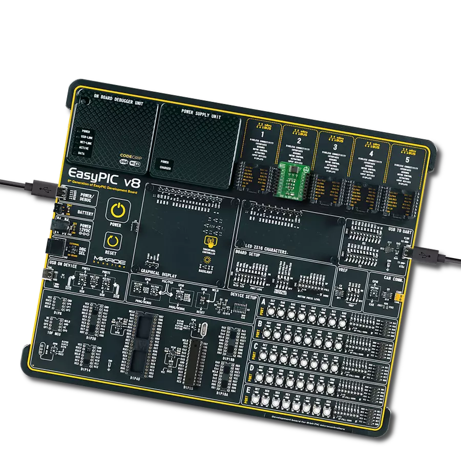
Development board
UNI-DS v8 is a development board specially designed for the needs of rapid development of embedded applications. It supports a wide range of microcontrollers, such as different STM32, Kinetis, TIVA, CEC, MSP, PIC, dsPIC, PIC32, and AVR MCUs regardless of their number of pins, and a broad set of unique functions, such as the first-ever embedded debugger/programmer over WiFi. The development board is well organized and designed so that the end-user has all the necessary elements, such as switches, buttons, indicators, connectors, and others, in one place. Thanks to innovative manufacturing technology, UNI-DS v8 provides a fluid and immersive working experience, allowing access anywhere and under any
circumstances at any time. Each part of the UNI-DS v8 development board contains the components necessary for the most efficient operation of the same board. An advanced integrated CODEGRIP programmer/debugger module offers many valuable programming/debugging options, including support for JTAG, SWD, and SWO Trace (Single Wire Output)), and seamless integration with the Mikroe software environment. Besides, it also includes a clean and regulated power supply module for the development board. It can use a wide range of external power sources, including a battery, an external 12V power supply, and a power source via the USB Type-C (USB-C) connector. Communication options such as USB-UART, USB
HOST/DEVICE, CAN (on the MCU card, if supported), and Ethernet is also included. In addition, it also has the well-established mikroBUS™ standard, a standardized socket for the MCU card (SiBRAIN standard), and two display options for the TFT board line of products and character-based LCD. UNI-DS v8 is an integral part of the Mikroe ecosystem for rapid development. Natively supported by Mikroe software tools, it covers many aspects of prototyping and development thanks to a considerable number of different Click boards™ (over a thousand boards), the number of which is growing every day.

Microcontroller Overview
MCU Card / MCU
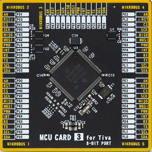
Type
8th Generation
Architecture
ARM Cortex-M4
MCU Memory (KB)
1024
Silicon Vendor
Texas Instruments
Pin count
128
RAM (Bytes)
262144
Used MCU Pins
mikroBUS™ mapper
Take a closer look
Click board™ Schematic
Step by step
Project assembly

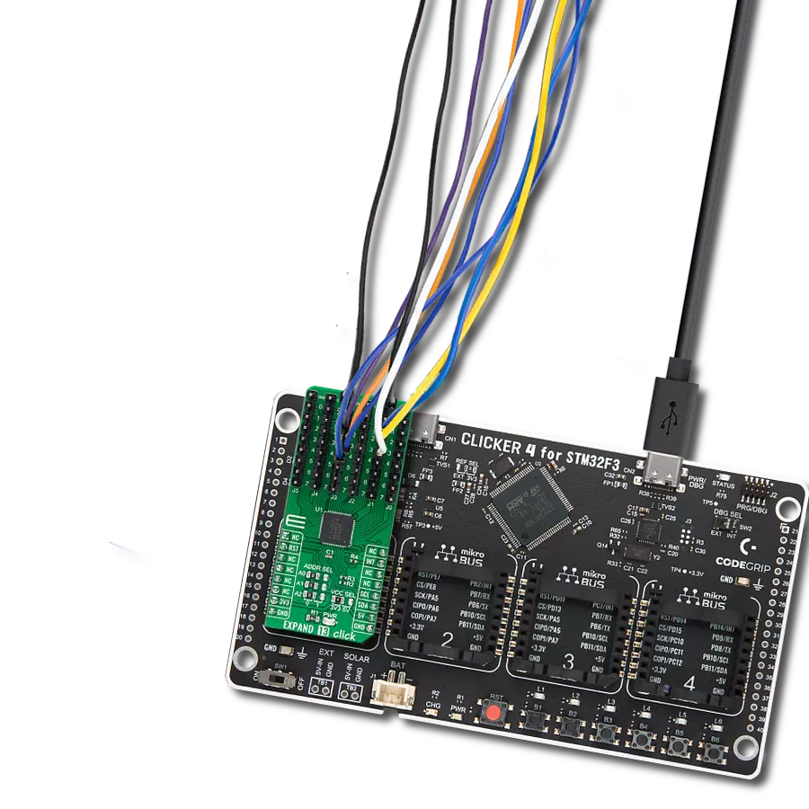
Start by selecting your development board and Click board™. Begin with the UNI-DS v8 as your development board.


Track your results in real time
Application Output
1. Application Output - In Debug mode, the 'Application Output' window enables real-time data monitoring, offering direct insight into execution results. Ensure proper data display by configuring the environment correctly using the provided tutorial.

2. UART Terminal - Use the UART Terminal to monitor data transmission via a USB to UART converter, allowing direct communication between the Click board™ and your development system. Configure the baud rate and other serial settings according to your project's requirements to ensure proper functionality. For step-by-step setup instructions, refer to the provided tutorial.

3. Plot Output - The Plot feature offers a powerful way to visualize real-time sensor data, enabling trend analysis, debugging, and comparison of multiple data points. To set it up correctly, follow the provided tutorial, which includes a step-by-step example of using the Plot feature to display Click board™ readings. To use the Plot feature in your code, use the function: plot(*insert_graph_name*, variable_name);. This is a general format, and it is up to the user to replace 'insert_graph_name' with the actual graph name and 'variable_name' with the parameter to be displayed.

Software Support
Library Description
This library contains API for Analog MUX Click driver.
Key functions:
analogmux_get_voltage- Generic read voltage functionanalogmux_set_channel- This function sets the active channel on the MUX.
Open Source
Code example
The complete application code and a ready-to-use project are available through the NECTO Studio Package Manager for direct installation in the NECTO Studio. The application code can also be found on the MIKROE GitHub account.
/*!
 * \file
 * \brief AnalogMUX Click example
 *
 * # Description
 * This example showcases how to initialize, configure and use the Analog MUX Click module.
 * The Click switches one of the 16 inputs to output so the adc value of that input
 * can be read on the COM (AN) pin. The RST, PWM, CS and INT are used as control output pins.
 *
 * The demo application is composed of two sections :
 *
 * ## Application Init
 * This function initializes and configures the logger and Click modules.
 *
 * ## Application Task
 * This function reads ADC value and voltage from channel 0 (AN0) and shows the results
 * on the USB UART every 2 seconds.
 *
 * \author MikroE Team
 *
 */
// ------------------------------------------------------------------- INCLUDES

#include "board.h"
#include "log.h"
#include "analogmux.h"

// ------------------------------------------------------------------ VARIABLES

static analogmux_t analogmux;
static log_t logger;

// ------------------------------------------------------ APPLICATION FUNCTIONS

void application_init ( void )
{
    log_cfg_t log_cfg;
    analogmux_cfg_t cfg;

    /**
     * Logger initialization.
     * Default baud rate: 115200
     * Default log level: LOG_LEVEL_DEBUG
     * @note If USB_UART_RX and USB_UART_TX
     * are defined as HAL_PIN_NC, you will
     * need to define them manually for log to work.
     * See @b LOG_MAP_USB_UART macro definition for detailed explanation.
     */
    LOG_MAP_USB_UART( log_cfg );
    log_init( &logger, &log_cfg );
    Delay_100ms( );
    log_info( &logger, "---- Application Init ----" );

    //  Click initialization.

    analogmux_cfg_setup( &cfg );
    ANALOGMUX_MAP_MIKROBUS( cfg, MIKROBUS_1 );
    analogmux_init( &analogmux, &cfg );

    analogmux_set_channel( &analogmux, ANALOGMUX_CHANNEL_0 );
    log_printf( &logger, " Channel 0 enabled\r\n" );
    log_printf( &logger, " -------------------\r\n" );
}

void application_task ( void )
{
    uint16_t tmp;
    float val;

    tmp = analogmux_generic_read( &analogmux );

    log_printf( &logger, " ADC value : %u\r\n", tmp );

    val = analogmux_generic_read_voltage( &analogmux );

    log_printf( &logger, " Voltage: %.3f mV\r\n", val );
    log_printf( &logger, " -------------------\r\n" );

    Delay_ms ( 1000 );
    Delay_ms ( 1000 );
}

int main ( void )
{
    /* Do not remove this line or clock might not be set correctly. */
    #ifdef PREINIT_SUPPORTED
    preinit();
    #endif

    application_init( );

    for ( ; ; )
    {
        application_task( );
    }

    return 0;
}

// ------------------------------------------------------------------------ END