Ensure instant access and consistent reliability of your data using CY14B101Q and TM4C129ENCPDT
Instantaneous data security: nvSRAM, where speed meets resilience

Published Oct 28, 2023
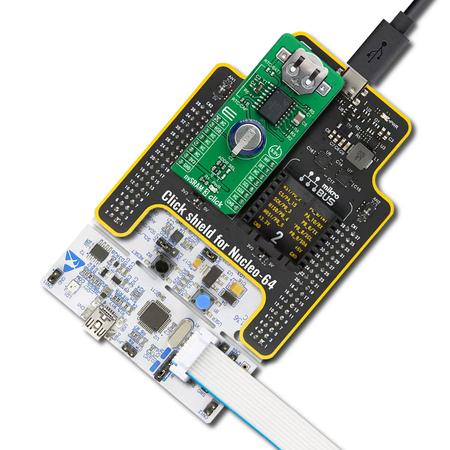
Click board™
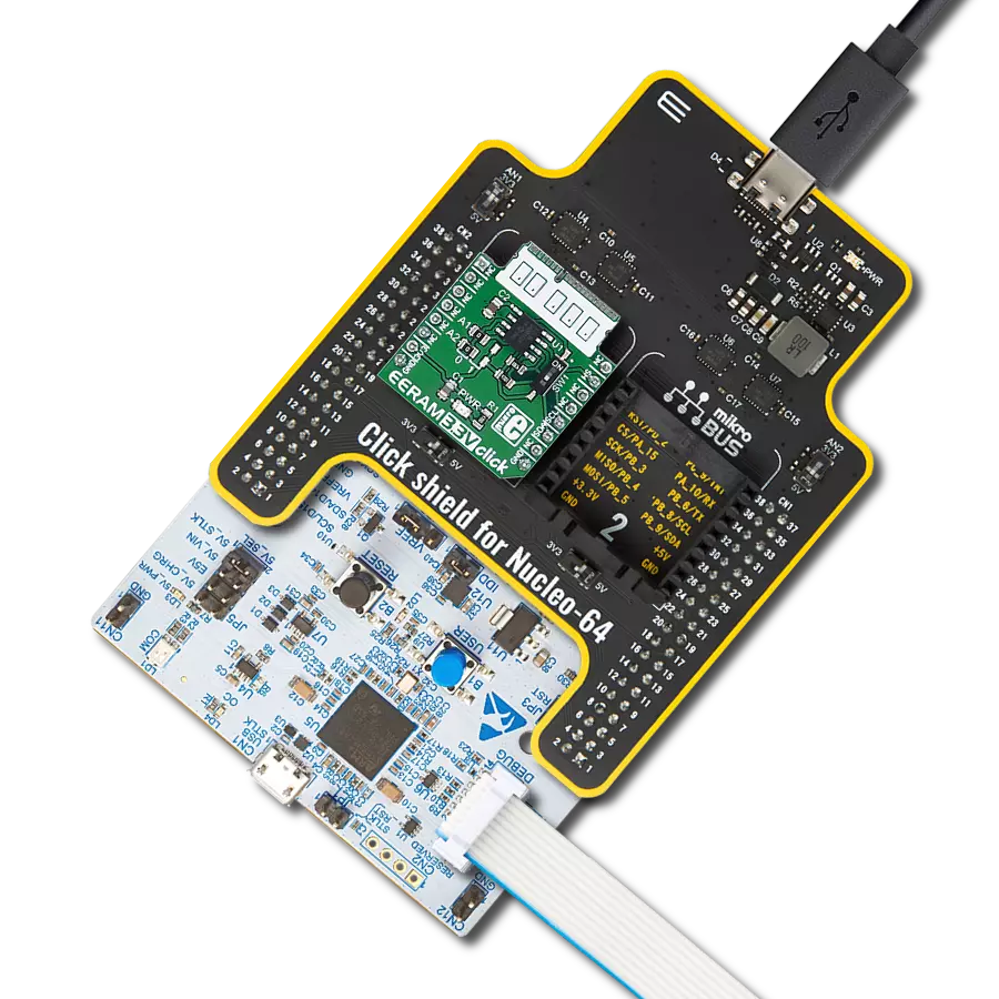
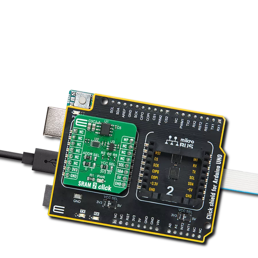
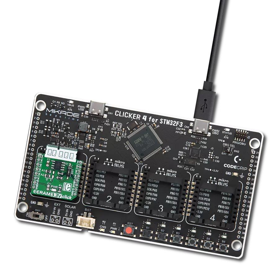
nvSRAM 2 Click
Dev. board
Fusion for Tiva v8
Compiler
NECTO Studio
MCU
TM4C129ENCPDT
Experience data security in a flash with the speed of SRAM and the resilience of non-volatile technology in our nvSRAM
A
A
Hardware Overview
How does it work?
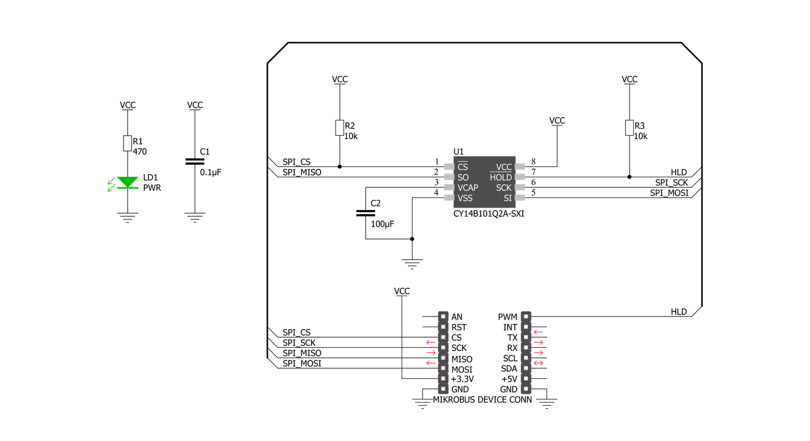
nvSRAM 2 Click is based on the CY14B101Q, a 1-Mbit nvSRAM organized as 128K words of 8 bits, each with a nonvolatile element in each memory cell from Infineon. The nvSRAM specifies one million endurance cycles for nonvolatile cells with data retention of a minimum of 20 years. All the reads and writes to nvSRAM happen to the SRAM, which gives nvSRAM the unique capability to handle infinite writes to the memory. Besides, the benefit of nvSRAM over serial EEPROMs is that all reads and writes to nvSRAM are performed at the SPI speed with zero cycle delay. Therefore, no wait time is required after any of the memory accesses. In the event of system power loss, data from the SRAM is transferred to its nonvolatile cell using energy stored in a capacitor labeled as C2.
During the Power-Up, data from the nonvolatile cell is recalled automatically in the SRAM array and available to the user. During the Power-Down, the endurance cycle is consumed only when data transfer happens from the SRAM cells to nonvolatile cells. The memory can be accessed through a standard SPI interface that enables high clock speeds up to 40 MHz with zero cycle delay read and write cycles. It also supports the two most common modes, SPI Mode 0 and 3, and 104 MHz SPI access speed with special instructions for the read operation. The CY14B101Q uses the standard SPI opcodes for memory access. In addition to the general SPI instructions for reading and writing, it provides four special instructions: STORE, RECALL, AutoStore Disable (ASDISB), and
AutoStore Enable (ASENB). In addition to this, the nvSRAM 2 Click also has an additional HOLD pin, routed to the PWM pin of the mikroBUS™ socket labeled as HLD, used to pause the serial communication with the device without having to stop the operation of the write status register, programming, or erasing in progress. This Click board™ can be operated only with a 3.3V logic voltage level. The board must perform appropriate logic voltage level conversion before using MCUs with different logic levels. Also, it comes equipped with a library containing functions and an example code that can be used as a reference for further development.

Features overview
Development board
Fusion for TIVA v8 is a development board specially designed for the needs of rapid development of embedded applications. It supports a wide range of microcontrollers, such as different 32-bit ARM® Cortex®-M based MCUs from Texas Instruments, regardless of their number of pins, and a broad set of unique functions, such as the first-ever embedded debugger/programmer over a WiFi network. The development board is well organized and designed so that the end-user has all the necessary elements, such as switches, buttons, indicators, connectors, and others, in one place. Thanks to innovative manufacturing technology, Fusion for TIVA v8 provides a fluid and immersive working experience, allowing access
anywhere and under any circumstances at any time. Each part of the Fusion for TIVA v8 development board contains the components necessary for the most efficient operation of the same board. An advanced integrated CODEGRIP programmer/debugger module offers many valuable programming/debugging options, including support for JTAG, SWD, and SWO Trace (Single Wire Output)), and seamless integration with the Mikroe software environment. Besides, it also includes a clean and regulated power supply module for the development board. It can use a wide range of external power sources, including a battery, an external 12V power supply, and a power source via the USB Type-C (USB-C) connector.
Communication options such as USB-UART, USB HOST/DEVICE, CAN (on the MCU card, if supported), and Ethernet is also included. In addition, it also has the well-established mikroBUS™ standard, a standardized socket for the MCU card (SiBRAIN standard), and two display options for the TFT board line of products and character-based LCD. Fusion for TIVA v8 is an integral part of the Mikroe ecosystem for rapid development. Natively supported by Mikroe software tools, it covers many aspects of prototyping and development thanks to a considerable number of different Click boards™ (over a thousand boards), the number of which is growing every day.

Microcontroller Overview
MCU Card / MCU
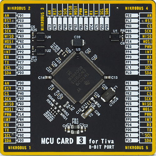
Type
8th Generation
Architecture
ARM Cortex-M4
MCU Memory (KB)
1024
Silicon Vendor
Texas Instruments
Pin count
128
RAM (Bytes)
262144
Used MCU Pins
mikroBUS™ mapper
Take a closer look
Click board™ Schematic
Step by step
Project assembly

Start by selecting your development board and Click board™. Begin with the Fusion for Tiva v8 as your development board.


Track your results in real time
Application Output
1. Application Output - In Debug mode, the 'Application Output' window enables real-time data monitoring, offering direct insight into execution results. Ensure proper data display by configuring the environment correctly using the provided tutorial.

2. UART Terminal - Use the UART Terminal to monitor data transmission via a USB to UART converter, allowing direct communication between the Click board™ and your development system. Configure the baud rate and other serial settings according to your project's requirements to ensure proper functionality. For step-by-step setup instructions, refer to the provided tutorial.

3. Plot Output - The Plot feature offers a powerful way to visualize real-time sensor data, enabling trend analysis, debugging, and comparison of multiple data points. To set it up correctly, follow the provided tutorial, which includes a step-by-step example of using the Plot feature to display Click board™ readings. To use the Plot feature in your code, use the function: plot(*insert_graph_name*, variable_name);. This is a general format, and it is up to the user to replace 'insert_graph_name' with the actual graph name and 'variable_name' with the parameter to be displayed.

Software Support
Library Description
This library contains API for nvSRAM 2 Click driver.
Key functions:
nvsram2_hold- The function enables hold operation by setting the state of the HOLD ( PWM ) pin depending on the function argument.nvsram2_set_cmd-The function sends desired command to the CY14B101Q2A memory on nvSRAM 2 click board.nvsram2_read_id- The function performs the device ID read of the CY14B101Q2A memory on nvSRAM 2 click board.
Open Source
Code example
The complete application code and a ready-to-use project are available through the NECTO Studio Package Manager for direct installation in the NECTO Studio. The application code can also be found on the MIKROE GitHub account.
/*!
 * @file main.c
 * @brief nvSRAM2 Click example
 *
 * # Description
 * This is an example using nvSRAM 2 Click based on CY14B101Q which is combines a 1-Mbit nvSRAM with a
 * nonvolatile element in each memory cell with serial SPI interface. The memory is organized as 128K words of 8 bits each.
 *
 * The demo application is composed of two sections :
 *
 * ## Application Init
 * Initializes SPI and UART LOG, sets CS and PWM pins as outputs.
 * Disables hold, sets write enable latch, targets the memory address at 12345 ( 0x00003039 )
 * for burst write starting point and writes data which is also displayed on the log.
 *
 * ## Application Task
 * This is an example that demonstrates the use of the nvSRAM 2 Click board. In this example, the data is read from
 * the targeted memory address. The results are being sent to the Usart Terminal. This task repeats every 5 sec.
 *
 * @author Jelena Milosavljevic
 *
 */

#include "board.h"
#include "log.h"
#include "nvsram2.h"

static nvsram2_t nvsram2;
static log_t logger;
static char demo_data[ 9 ] = { 'm', 'i', 'k', 'r', 'o', 'E', 13 ,10 , 0 };
static char rx_data[ 9 ];
static uint32_t memory_addr;

void application_init ( void ) {
    log_cfg_t log_cfg;               /**< Logger config object. */
    nvsram2_cfg_t nvsram2_cfg;       /**< Click config object. */

    /**
     * Logger initialization.
     * Default baud rate: 115200
     * Default log level: LOG_LEVEL_DEBUG
     * @note If USB_UART_RX and USB_UART_TX
     * are defined as HAL_PIN_NC, you will
     * need to define them manually for log to work.
     * See @b LOG_MAP_USB_UART macro definition for detailed explanation.
     */
    LOG_MAP_USB_UART( log_cfg );
    log_init( &logger, &log_cfg );
    Delay_ms ( 100 );
    log_info( &logger, " Application Init " );

    // Click initialization.

    nvsram2_cfg_setup( &nvsram2_cfg );
    NVSRAM2_MAP_MIKROBUS( nvsram2_cfg, MIKROBUS_1 );
    err_t init_flag  = nvsram2_init( &nvsram2, &nvsram2_cfg );
    if ( SPI_MASTER_ERROR == init_flag ) {

        log_error( &logger, " Application Init Error. " );
        log_info( &logger, " Please, run program again... " );

        for ( ; ; );
    }

    nvsram2_default_cfg ( &nvsram2 );
    log_info( &logger, " Application Task " );

    memory_addr = 12345;

    nvsram2_burst_write( &nvsram2, memory_addr, demo_data, 9 );
    log_printf( &logger, "-----------------------\r\n" );
    log_printf( &logger, "-> Write data : %s \r\n", demo_data );
    Delay_ms ( 100 );
}

void application_task ( void ) {
    nvsram2_burst_read( &nvsram2, memory_addr, rx_data, 9 );
    log_printf( &logger, "-----------------------\r\n"  );
    log_printf( &logger, "<- Read data  : %s \r\n", rx_data );
    Delay_ms ( 1000 );
    Delay_ms ( 1000 );
    Delay_ms ( 1000 );
    Delay_ms ( 1000 );
    Delay_ms ( 1000 );
}

int main ( void )
{
    /* Do not remove this line or clock might not be set correctly. */
    #ifdef PREINIT_SUPPORTED
    preinit();
    #endif

    application_init( );

    for ( ; ; )
    {
        application_task( );
    }

    return 0;
}

// ------------------------------------------------------------------------ END