Adjust every aspect of your systems easily with PT10MV11-103A2020-S and PIC18F97J60
Fine-tune your world: Meet the precision of trimmer potentiometers

Published Oct 10, 2023
Click board™
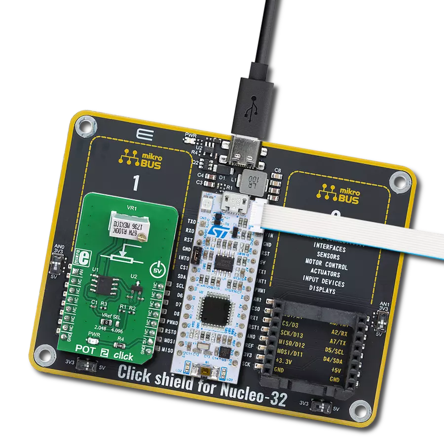
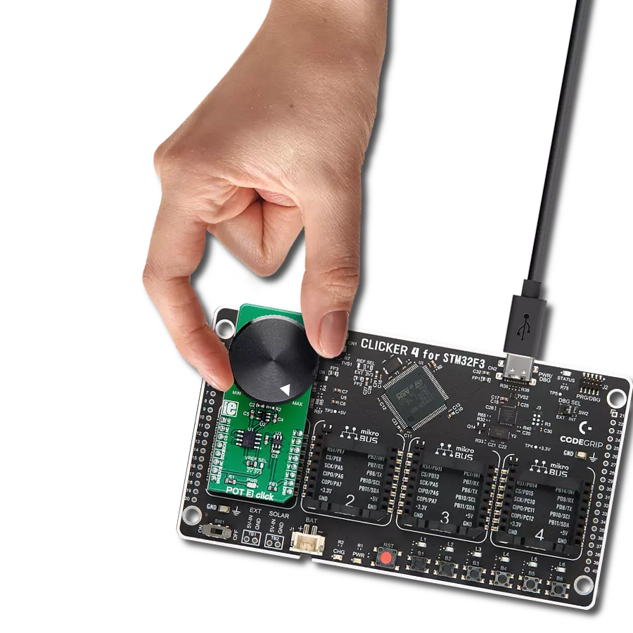
POT Click
Dev. board
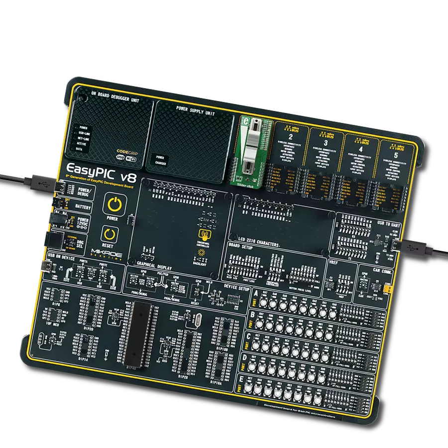
UNI-DS v8
Compiler
NECTO Studio
MCU
PIC18F97J60
We're dedicated to providing you with the tools to fine-tune and optimize your devices for better performance and accuracy, and our trimmer potentiometers are at the heart of this dedication
A
A
Hardware Overview
How does it work?
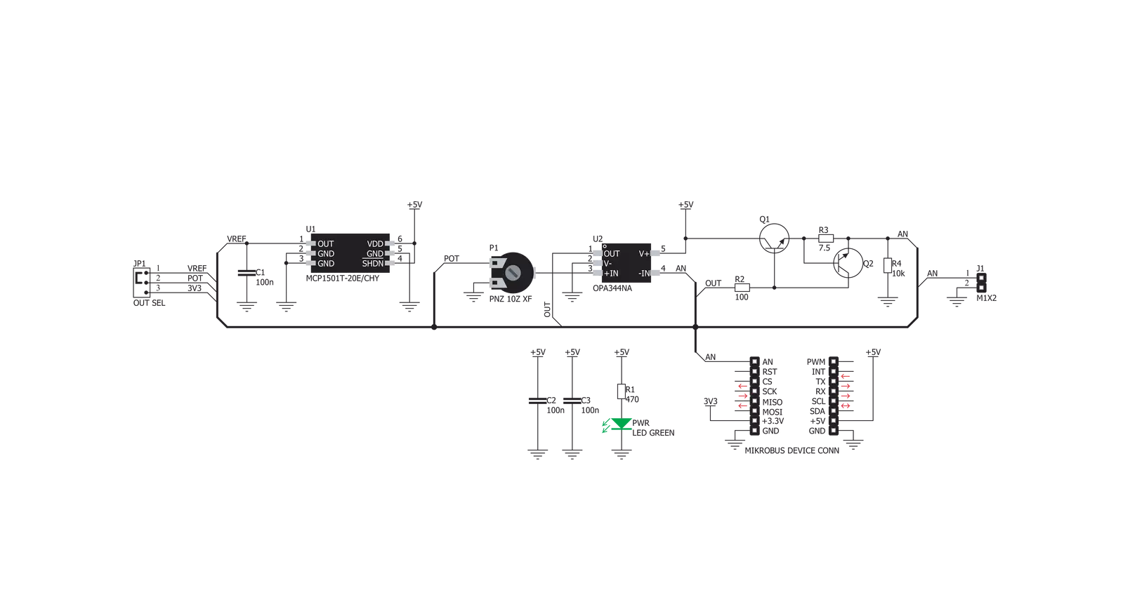
POT Click is based on the MCP1501, a precision voltage reference IC from Microchip is used to provide the voltage of 2.048V. This voltage is routed to the small SMD jumper labeled as OUT SEL. By moving the jumper to the REF position, 2.048V will be applied to one end of the potentiometer. Otherwise, the potentiometer will be connected to the 3.3V rail of the mikroBUS™. The other end of the potentiometer is tied to GND, allowing to select voltage either from 0 to 2.048V range (VREF) or from 0 to 3.3V range. The adjustable voltage is available on both AN pin of the mikroBUS™ and 1x2-pin header on the upper edge of the Click board™, which is labeled as VOUT. The potentiometer itself is labeled as PT10MV11-103A2020-S. It is a high-quality potentiometer from Piher Sensing Systems. This company is otherwise known for their high-quality potentiometers, used in many industries. The
potentiometer has a carbon-based resistive surface with the resistance of 10 kΩ. It is a single-turn linear potentiometer, with 50% of resistance achieved when in the middle position. It has 10mm in diameter. Its turning knob is not fixed: the potentiometer has a hole with flat surfaces instead (hexagonal shape), and a small pole with the matching shape can be inserted. This makes possible using both fingers and some other precision tool (screwdriver, hex keys, and more). The output of the potentiometer is fed to the non-inverting input of the OPA344, a rail-to-rail single supply operational amplifier, from Texas Instruments. This operational amplifier is a perfect choice for this design, as it allows rail-to-rail operation, uses a single power supply of 5V, and has a stable unity gain. The OPA344 is used as a buffer, providing a constant input and output impedance. Without buffer, variable impedance
would affect the reference voltage. The reference voltage can provide less than 10 mA, with the significant voltage drop for output currents exceeding 2 mA. Therefore, the OPA344 ensures good stability of the circuit. The current output of this Click board™ is limited by the circuit at the output, which consists of two BJT transistors. When the output load is too large, a voltage drop will appear across the base-emitter resistor on the Q2 transistor, which in turn starts to conduct, reducing the voltage across the feedback loop, limiting the max current this way. Q1 transistor is otherwise used to provide enough current to the output load, preventing the damage to the buffer and the rest of the circuit. Therefore, in the case of short circuit, this transistor will start dissipating heat. It is dimensioned so that it can withstand short circuit on the output. The connected load can draw up to 100mA of current.

Features overview
Development board
UNI-DS v8 is a development board specially designed for the needs of rapid development of embedded applications. It supports a wide range of microcontrollers, such as different STM32, Kinetis, TIVA, CEC, MSP, PIC, dsPIC, PIC32, and AVR MCUs regardless of their number of pins, and a broad set of unique functions, such as the first-ever embedded debugger/programmer over WiFi. The development board is well organized and designed so that the end-user has all the necessary elements, such as switches, buttons, indicators, connectors, and others, in one place. Thanks to innovative manufacturing technology, UNI-DS v8 provides a fluid and immersive working experience, allowing access anywhere and under any
circumstances at any time. Each part of the UNI-DS v8 development board contains the components necessary for the most efficient operation of the same board. An advanced integrated CODEGRIP programmer/debugger module offers many valuable programming/debugging options, including support for JTAG, SWD, and SWO Trace (Single Wire Output)), and seamless integration with the Mikroe software environment. Besides, it also includes a clean and regulated power supply module for the development board. It can use a wide range of external power sources, including a battery, an external 12V power supply, and a power source via the USB Type-C (USB-C) connector. Communication options such as USB-UART, USB
HOST/DEVICE, CAN (on the MCU card, if supported), and Ethernet is also included. In addition, it also has the well-established mikroBUS™ standard, a standardized socket for the MCU card (SiBRAIN standard), and two display options for the TFT board line of products and character-based LCD. UNI-DS v8 is an integral part of the Mikroe ecosystem for rapid development. Natively supported by Mikroe software tools, it covers many aspects of prototyping and development thanks to a considerable number of different Click boards™ (over a thousand boards), the number of which is growing every day.

Microcontroller Overview
MCU Card / MCU
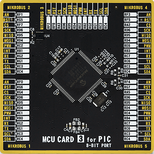
Type
8th Generation
Architecture
PIC
MCU Memory (KB)
128
Silicon Vendor
Microchip
Pin count
100
RAM (Bytes)
3808
Used MCU Pins
mikroBUS™ mapper
Take a closer look
Click board™ Schematic
Step by step
Project assembly

Start by selecting your development board and Click board™. Begin with the UNI-DS v8 as your development board.


Software Support
Library Description
This library contains API for POT Click driver.
Key functions:
pot_read_an_pin_value- This function reads results of AD conversion of the AN pinpot_read_an_pin_voltage- This function reads results of AD conversion of the AN pin and converts them to proportional voltage level
Open Source
Code example
The complete application code and a ready-to-use project are available through the NECTO Studio Package Manager for direct installation in the NECTO Studio. The application code can also be found on the MIKROE GitHub account.
/*!
 * \file
 * \brief Pot Click example
 *
 * # Description
 * Click board with the accurate selectable reference voltage output.
 *
 * The demo application is composed of two sections :
 *
 * ## Application Init
 * Performs logger and Click initialization.
 *
 * ## Application Task
 * Reads and displays on the USB UART the voltage level measured from AN pin.
 *
 * \author Nemanja Medakovic
 *
 */
// ------------------------------------------------------------------- INCLUDES

#include "board.h"
#include "log.h"
#include "pot.h"

// ------------------------------------------------------------------ VARIABLES

static pot_t pot;
static log_t logger;

// ------------------------------------------------------ APPLICATION FUNCTIONS

void application_init ( void )
{
    log_cfg_t log_cfg;  /**< Logger config object. */
    pot_cfg_t pot_cfg;  /**< Click config object. */

    /**
     * Logger initialization.
     * Default baud rate: 115200
     * Default log level: LOG_LEVEL_DEBUG
     * @note If USB_UART_RX and USB_UART_TX
     * are defined as HAL_PIN_NC, you will
     * need to define them manually for log to work.
     * See @b LOG_MAP_USB_UART macro definition for detailed explanation.
     */
    LOG_MAP_USB_UART( log_cfg );
    log_init( &logger, &log_cfg );
    log_info( &logger, " Application Init " );

    // Click initialization.
    pot_cfg_setup( &pot_cfg );
    POT_MAP_MIKROBUS( pot_cfg, MIKROBUS_1 );
    if ( ADC_ERROR == pot_init( &pot, &pot_cfg ) )
    {
        log_error( &logger, " Communication init." );
        for ( ; ; );
    }

    log_info( &logger, " Application Task " );
}

void application_task ( void )
{
    float voltage = 0;
    if ( POT_OK == pot_read_an_pin_voltage ( &pot, &voltage ) )
    {
        log_printf( &logger, " AN Voltage : %.3f[V]\r\n\n", voltage );
        Delay_ms ( 1000 );
    }
}

int main ( void )
{
    /* Do not remove this line or clock might not be set correctly. */
    #ifdef PREINIT_SUPPORTED
    preinit();
    #endif

    application_init( );

    for ( ; ; )
    {
        application_task( );
    }

    return 0;
}

// ------------------------------------------------------------------------ END