Experience the future of wireless charging with P9025AC and TM4C129ENCPDT
Power up without wires - Qi-ready and hassle-free!

Published Nov 02, 2023
Click board™
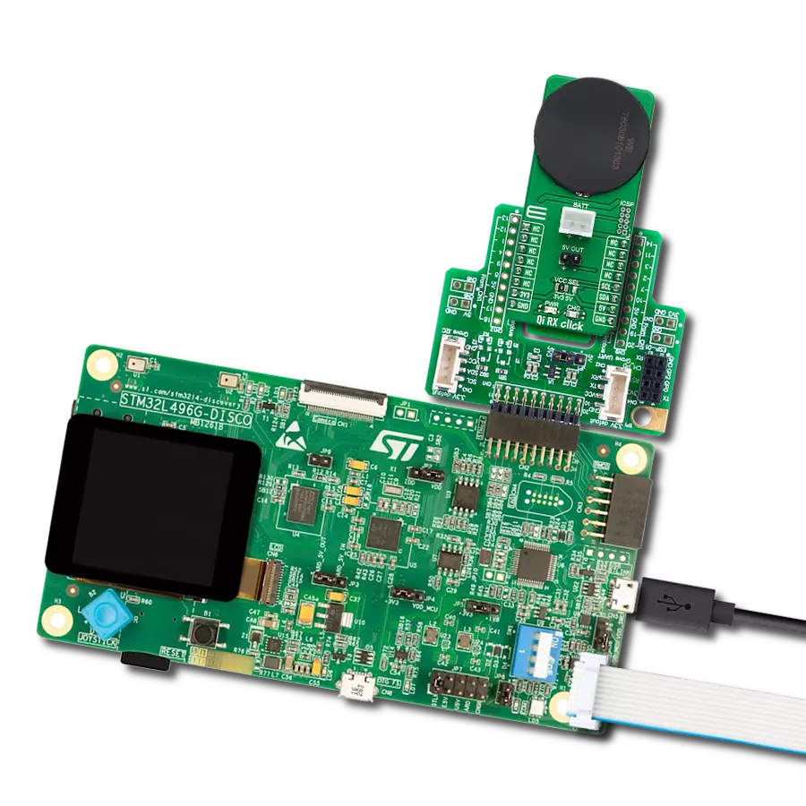
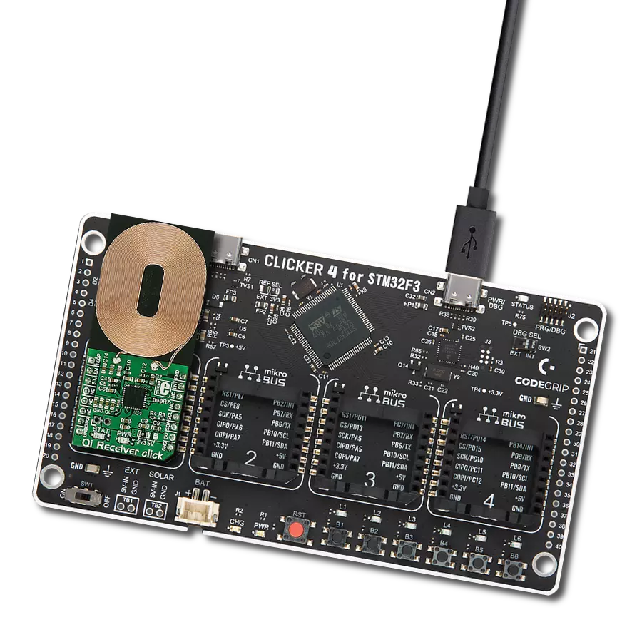
Qi Receiver Click
Dev. board
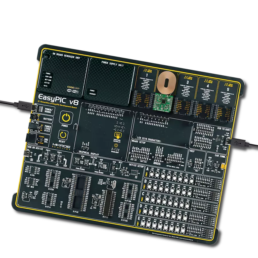
Fusion for Tiva v8
Compiler
NECTO Studio
MCU
TM4C129ENCPDT
Our Qi-compliant wireless power receiver empowers you to charge your devices with ease, making everyday life more convenient and clutter-free.
A
A
Hardware Overview
How does it work?
Qi Receiver Click is based on the P9025AC, a compact Qi-compliant wireless power receiver ideal for many portable applications looking to take advantage of wireless charging technology from Renesas. This Click board™ utilizes the principles of inductive coupling for wireless power transfer. It uses P9025AC's integrated synchronous full-bridge rectifier and LDO output stage to convert the harvested wireless power signal from the Wurth Electronik's 760308103205 wireless power coil into a regulated 5.3V/1A output (unpopulated OUT header) suitable to charge a battery or power a system directly. Its operation automatically initiates WPC AC modulation communication protocols with optimal efficiency. In addition, it employs advanced Foreign Object Detection (FOD) techniques to safeguard the system. This Click board™ relies on the wireless power transfer standard, developed by the Wireless Power Consortium (WPC), to provide and monitor current and voltage. This standard involves digital communication to transmit the information to the charging pad. Depending on the received information packets, the charging pad regulates the variable magnetic field's strength, generating more or less power on the receiver coil. The P9025AC includes control
circuitry to transmit WPC-compliant message packets to the base station. When Qi Receiver Click is placed on a WPS Qi-compliant charging pad, it responds to the transmitter's "ping" signal by rectifying the AC power from the transmitter. During the "ping" phase, the rectifier provides about 5V, and an internal linear voltage regulator provides the supply voltage for the digital section of the P9025AC, enabling the Qi protocol communication so that the receiver can synchronize with the charging pad. After the initial synchronization, the system enters the Power Transfer state, and the actual power transfer process is started, monitored via the ST pin routed to the CS pin of the mikroBUS™ socket and indicated by the red Status LED indicator. Termination of the charging process is indicated by the END pin routed to the PWM pin of the mikroBUS™ socket. To simplify the Power-up and usage of the Qi Receiver Click board™, place the Qi Receiver Click with the inductive coil facing down toward the transmitter and verify that the STAT LED is illuminated, which means that the power is being transferred. After that, connect the load to the output pads. One special feature of this device is the possibility to detect foreign metal objects in the charging field, which can be heated
up by the eddy currents generated inside, with heat translated into a power loss. This state can be especially problematic if the object is a part of the power harvesting device. To overcome this problem, the P9025AC employs advanced Foreign Object Detection (FOD) techniques to safeguard the system, accurately measure its received power, and compensate for its known losses. Qi Receiver Click communicates with MCU using the standard I2C 2-Wire interface. The P9025AC can be enabled/disabled through the EN pin routed to the RST pin of the mikroBUS™ socket, hence offering a switch operation to turn ON/OFF power delivery to the chip. Overvoltage, overcurrent, and thermal shutdown features are also supported. Suppose any of these conditions occur on the output terminal. In that case, the LDO gets shut down, the charging pad stops transmitting the power, and the host MCU is notified of this situation via an interrupt signal. This Click board™ can operate with both 3.3V and 5V logic voltage levels selected via SMD jumper. This way, both 3.3V and 5V capable MCUs can use the communication lines properly. Also, this Click board™ comes equipped with a library containing easy-to-use functions and an example code that can be used as a reference for further development.

Features overview
Development board
Fusion for TIVA v8 is a development board specially designed for the needs of rapid development of embedded applications. It supports a wide range of microcontrollers, such as different 32-bit ARM® Cortex®-M based MCUs from Texas Instruments, regardless of their number of pins, and a broad set of unique functions, such as the first-ever embedded debugger/programmer over a WiFi network. The development board is well organized and designed so that the end-user has all the necessary elements, such as switches, buttons, indicators, connectors, and others, in one place. Thanks to innovative manufacturing technology, Fusion for TIVA v8 provides a fluid and immersive working experience, allowing access
anywhere and under any circumstances at any time. Each part of the Fusion for TIVA v8 development board contains the components necessary for the most efficient operation of the same board. An advanced integrated CODEGRIP programmer/debugger module offers many valuable programming/debugging options, including support for JTAG, SWD, and SWO Trace (Single Wire Output)), and seamless integration with the Mikroe software environment. Besides, it also includes a clean and regulated power supply module for the development board. It can use a wide range of external power sources, including a battery, an external 12V power supply, and a power source via the USB Type-C (USB-C) connector.
Communication options such as USB-UART, USB HOST/DEVICE, CAN (on the MCU card, if supported), and Ethernet is also included. In addition, it also has the well-established mikroBUS™ standard, a standardized socket for the MCU card (SiBRAIN standard), and two display options for the TFT board line of products and character-based LCD. Fusion for TIVA v8 is an integral part of the Mikroe ecosystem for rapid development. Natively supported by Mikroe software tools, it covers many aspects of prototyping and development thanks to a considerable number of different Click boards™ (over a thousand boards), the number of which is growing every day.

Microcontroller Overview
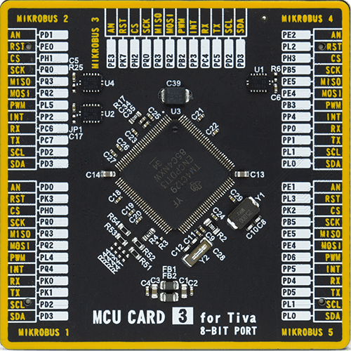
MCU Card / MCU
Type
8th Generation
Architecture
ARM Cortex-M4
MCU Memory (KB)
1024
Silicon Vendor
Texas Instruments
Pin count
128
RAM (Bytes)
262144
Used MCU Pins
mikroBUS™ mapper
Take a closer look
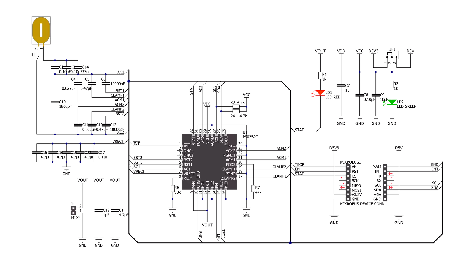
Click board™ Schematic
Step by step
Project assembly

Start by selecting your development board and Click board™. Begin with the Fusion for Tiva v8 as your development board.


Software Support
Library Description
This library contains API for Qi Receiver Click driver.
Key functions:
qireceiver_read_voltage- Function is used to measure current voltage in volt.qireceiver_read_current- Function is used to measure current amperage in mA.qireceiver_read_freq- Function is used to measure current frequency in hertz.qireceiver_dev_enable- Function is used to enable the device.
Open Source
Code example
The complete application code and a ready-to-use project are available through the NECTO Studio Package Manager for direct installation in the NECTO Studio. The application code can also be found on the MIKROE GitHub account.
/*!
 * \file
 * \brief QiReceiver Click example
 *
 * # Description
 * This application reads voltage, current and frequency.
 *
 * The demo application is composed of two sections :
 *
 * ## Application Init
 *  Initalizes I2C driver, enables the device and makes an initial log.
 *
 * ## Application Task
 * This is an example that shows the most important
 * functions that Qi Receiver Click has, it mesures current voltage, amperage and frequency.
 *
 * ## Note
 * Click board needs to have external power ( Qi transmitter ) in order to work, otherwise I2C communication won't work.
 * If Qi Transmitter is removed from Click board it will stop working, if you return it you should restart your application.
 * You will now when Click board has power and is ready to start application when red STAT led is on, when it's off I2C communication won't work.
 *
 * \author MikroE Team
 *
 */
// ------------------------------------------------------------------- INCLUDES

#include "board.h"
#include "log.h"
#include "qireceiver.h"

// ------------------------------------------------------------------ VARIABLES

static qireceiver_t qireceiver;
static log_t logger;

// ------------------------------------------------------ APPLICATION FUNCTIONS

void application_init ( void )
{
    log_cfg_t log_cfg;
    qireceiver_cfg_t cfg;

    /**
     * Logger initialization.
     * Default baud rate: 115200
     * Default log level: LOG_LEVEL_DEBUG
     * @note If USB_UART_RX and USB_UART_TX
     * are defined as HAL_PIN_NC, you will
     * need to define them manually for log to work.
     * See @b LOG_MAP_USB_UART macro definition for detailed explanation.
     */
    LOG_MAP_USB_UART( log_cfg );
    log_init( &logger, &log_cfg );
    log_info( &logger, "---- Application Init ----" );

    //  Click initialization.

    qireceiver_cfg_setup( &cfg );
    QIRECEIVER_MAP_MIKROBUS( cfg, MIKROBUS_1 );
    qireceiver_init( &qireceiver, &cfg );

    Delay_ms ( 100 );
    qireceiver_dev_enable( &qireceiver );
    log_printf( &logger, "-----------------\r\n" );
    log_printf( &logger, "Qi Receiver Click\r\n" );
    log_printf( &logger, "-----------------\r\n" );
    Delay_ms ( 100 );
}

void application_task ( void )
{
    float voltage;
    float current;
    float freq;

    voltage = qireceiver_read_voltage( &qireceiver );
    log_printf( &logger, "Voltage : %.2f V\r\n", voltage );

    current = qireceiver_read_current( &qireceiver );
    log_printf( &logger, "Current : %.2f mA\r\n", current );

    freq = qireceiver_read_freq( &qireceiver );
    log_printf( &logger, "Frequency : %.2f Hz\r\n", freq );

    log_printf( &logger, "-----------------\r\n" );
    Delay_ms ( 1000 );
}

int main ( void )
{
    /* Do not remove this line or clock might not be set correctly. */
    #ifdef PREINIT_SUPPORTED
    preinit();
    #endif

    application_init( );

    for ( ; ; )
    {
        application_task( );
    }

    return 0;
}


// ------------------------------------------------------------------------ END
Additional Support
Resources
Category:Wireless Charging