Experience lightning-fast power/data sharing with STUSB4500 and STM32L496AG
Never run out of juice
Published Jul 22, 2025
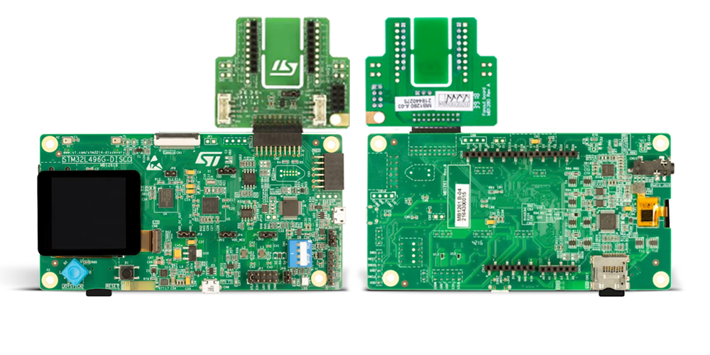
Click board™
USB-C Sink Click
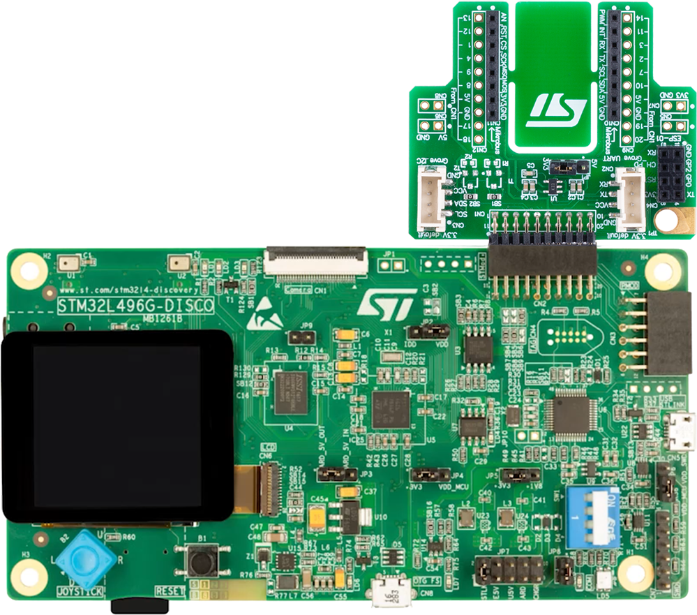
Dev. board
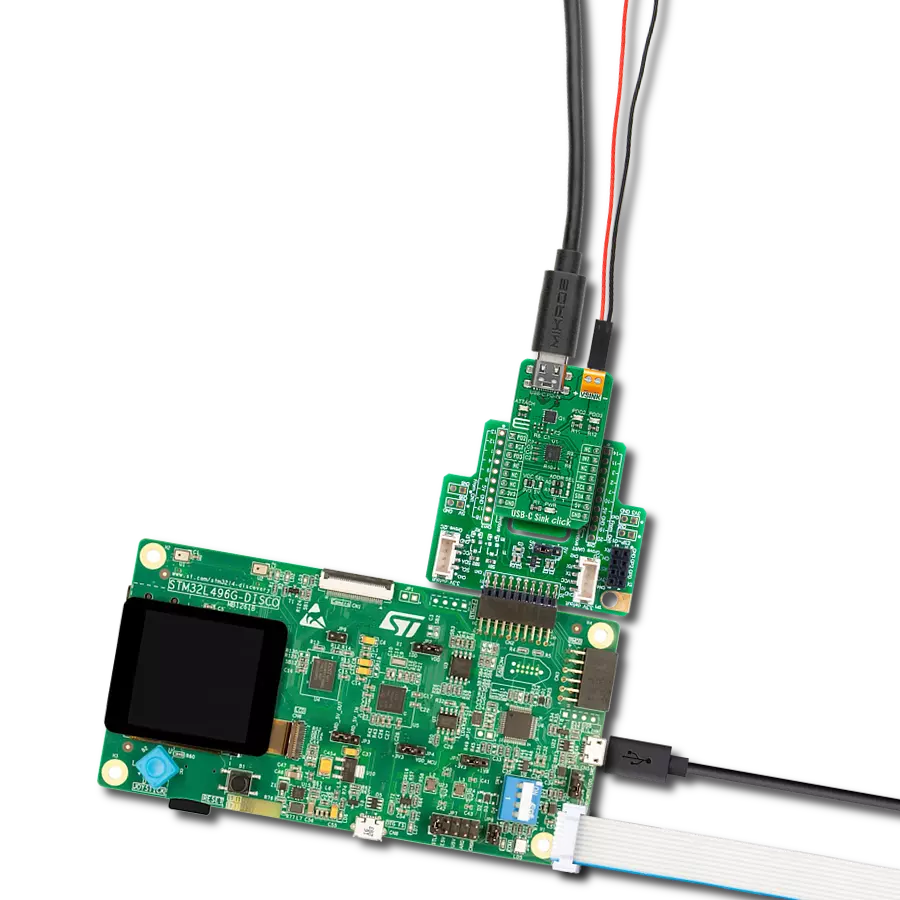
Discovery kit with STM32L496AG MCU
Compiler
NECTO Studio
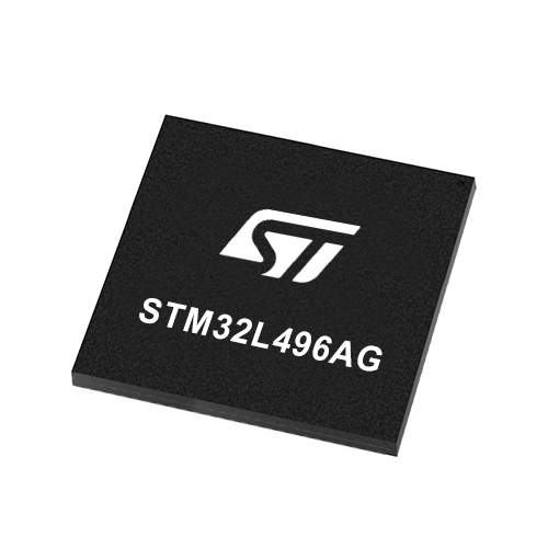
MCU
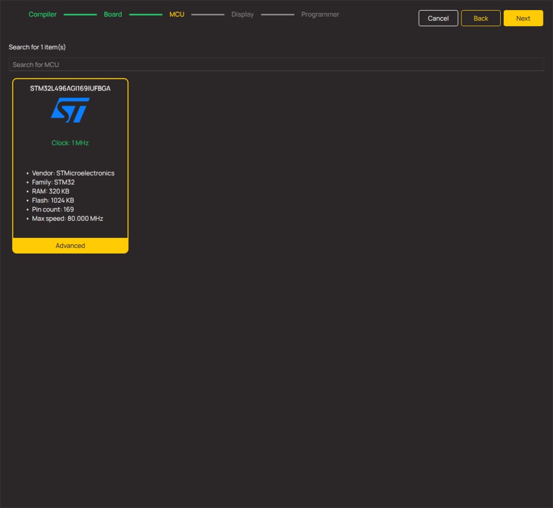
STM32L496AG
Say goodbye to low battery anxiety – our USB-C Sink guarantees your devices stay charged and ready for action.
A
A
Hardware Overview
How does it work?
USB-C Sink Click is based on the STUSB4500, a USB-C sink-only controller compatible with Power-Delivery (PD) from STMicroelectronics. Based on the default power profiles (PDO) configuration stored in internal non-volatile memory, the stand-alone controller STUSB4500 implements proprietary algorithms to negotiate a Power Delivery contract with a source without any internal or external software support (Auto-Run Mode), making it the ideal device for automatic High Power Profile charging, especially from a Dead Battery Power state. This Click board™ has the VBUS monitoring block that supervises from the VBUS_VS_DISCH input pin the VBUS voltage on the USB Type-C receptacle side. It is used to check that VBUS is within a valid voltage range to establish a correct Source-to-Sink connection and to enable a safe VBUS power path through the VBUS_EN_SNK pin. It detects unexpected VBUS voltage conditions, such as undervoltage or
overvoltage, relative to the valid VBUS voltage range. The STUSB4500 also has a pin that is asserted when a valid Source-to-Sink connection is established and when a connection to a debug accessory device is detected, presented visually with a blue LED labeled ATTACH. The STUSB4500 communicates with MCU using the standard I2C interface that supports transfers up to 400 Kbit/s (Fast Mode) to configure, control, and read the device's status. It also has the possibility of the USB Power Delivery communication over CC1 and CC2 configuration channel pins used for connection and attachment detection, plug orientation determination, and system configuration management across USB Type-C cables. Four 7-bit device address is available by default (0x28, 0x29, 0x2A, or 0x2B) depending on the setting of the address pin ADDR0 and ADDR1. The user programs these pins and determines the LSBs of the slave address, and it can be selected
by positioning the onboard SMD jumpers labeled as ADDR SEL. Additional functionality, such as Reset and 'Alert' interrupt, is provided and routed at RST and INT pins of the mikroBUS™ socket. The RST pin resets all analog signals, states machine, and reloads configuration, while an interrupt output labeled INT represents alarm output. Also, there are two additional green diodes associated with two pins on the mikroBUS™ socket (labeled as PO2 and PO3) that report by default the status of the USB power delivery contract negotiation with the source labeled as PDO2 and PDO3. This Click board™ can operate with either 3.3V or 5V logic voltage levels selected via the VCC SEL jumper. This way, both 3.3V and 5V capable MCUs can use the communication lines properly. Also, this Click board™ comes equipped with a library containing easy-to-use functions and an example code that can be used as a reference for further development.

Features overview
Development board
The 32L496GDISCOVERY Discovery kit serves as a comprehensive demonstration and development platform for the STM32L496AG microcontroller, featuring an Arm® Cortex®-M4 core. Designed for applications that demand a balance of high performance, advanced graphics, and ultra-low power consumption, this kit enables seamless prototyping for a wide range of embedded solutions. With its innovative energy-efficient
architecture, the STM32L496AG integrates extended RAM and the Chrom-ART Accelerator, enhancing graphics performance while maintaining low power consumption. This makes the kit particularly well-suited for applications involving audio processing, graphical user interfaces, and real-time data acquisition, where energy efficiency is a key requirement. For ease of development, the board includes an onboard ST-LINK/V2-1
debugger/programmer, providing a seamless out-of-the-box experience for loading, debugging, and testing applications without requiring additional hardware. The combination of low power features, enhanced memory capabilities, and built-in debugging tools makes the 32L496GDISCOVERY kit an ideal choice for prototyping advanced embedded systems with state-of-the-art energy efficiency.
Microcontroller Overview
MCU Card / MCU
Architecture
ARM Cortex-M4
MCU Memory (KB)
1024
Silicon Vendor
STMicroelectronics
Pin count
169
RAM (Bytes)
327680
Used MCU Pins
mikroBUS™ mapper
Take a closer look
Click board™ Schematic

Step by step
Project assembly
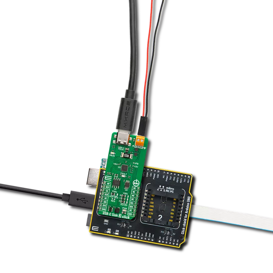
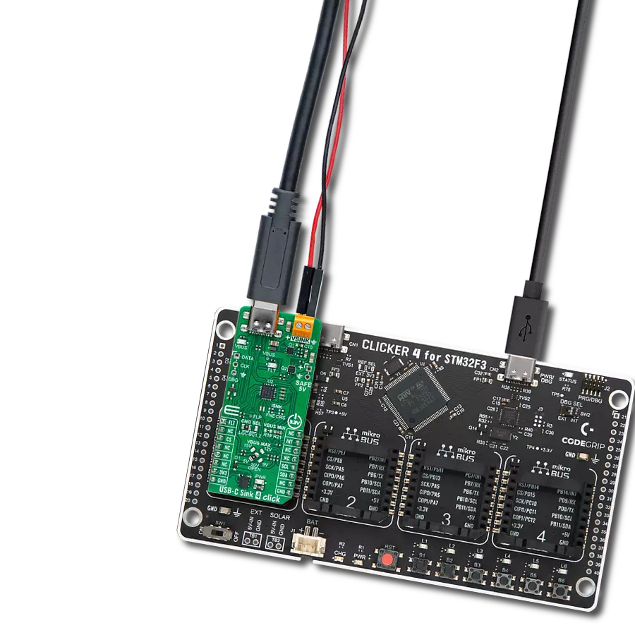
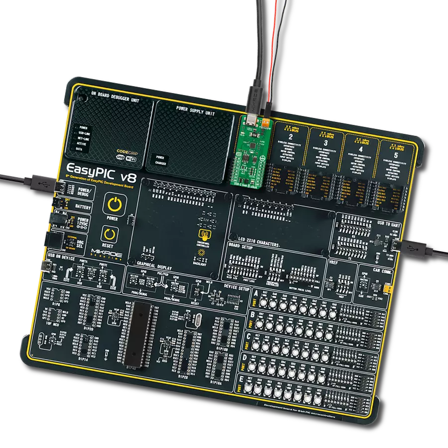
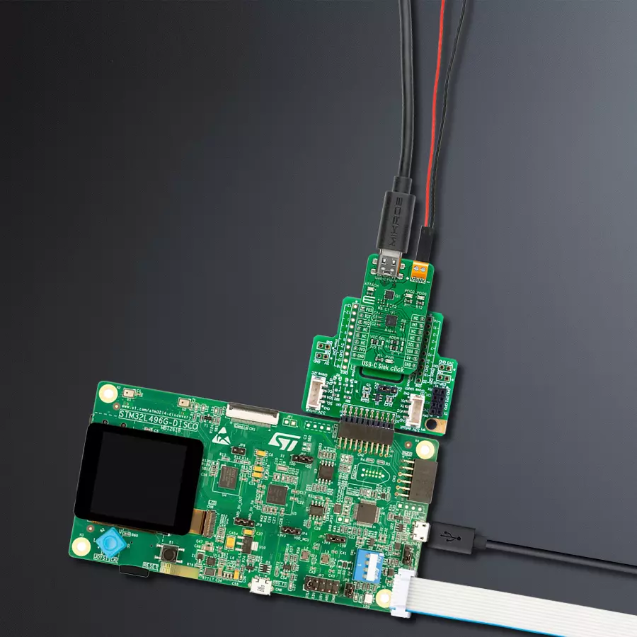
Start by selecting your development board and Click board™. Begin with the Discovery kit with STM32L496AG MCU as your development board.


Track your results in real time
Application Output
1. Application Output - In Debug mode, the 'Application Output' window enables real-time data monitoring, offering direct insight into execution results. Ensure proper data display by configuring the environment correctly using the provided tutorial.

2. UART Terminal - Use the UART Terminal to monitor data transmission via a USB to UART converter, allowing direct communication between the Click board™ and your development system. Configure the baud rate and other serial settings according to your project's requirements to ensure proper functionality. For step-by-step setup instructions, refer to the provided tutorial.

3. Plot Output - The Plot feature offers a powerful way to visualize real-time sensor data, enabling trend analysis, debugging, and comparison of multiple data points. To set it up correctly, follow the provided tutorial, which includes a step-by-step example of using the Plot feature to display Click board™ readings. To use the Plot feature in your code, use the function: plot(*insert_graph_name*, variable_name);. This is a general format, and it is up to the user to replace 'insert_graph_name' with the actual graph name and 'variable_name' with the parameter to be displayed.

Software Support
Library Description
This library contains API for USB-C Sink Click driver.
Key functions:
usbcsink_hw_reset- HW reset function.usbcsink_get_pdo2- Get PO2 pin state function.usbcsink_write_byte- Write byte function.
Open Source
Code example
The complete application code and a ready-to-use project are available through the NECTO Studio Package Manager for direct installation in the NECTO Studio. The application code can also be found on the MIKROE GitHub account.
/*!
 * @file main.c
 * @brief USBCSink Click example
 *
 * # Description
 * This is an example which demonstrates the use of USB-C Sink Click board.
 *
 * The demo application is composed of two sections :
 *
 * ## Application Init
 * Initialization driver enables - I2C,
 * set hw reset, set PDO2 profile and current value for PDO2 1.5A,
 * upload new data and reset device to write NVM settings to the STUSB450,
 * also write log.
 *
 * ## Application Task
 * USB-C Sink Click board can be used to read the Power Data Objects (PDO)
 * highest priority profile:
 * PDO1 :  5V,
 * PDO2 : 12V,
 * PDO3 : 20V.
 * All data logs write on USB uart changes for every 5 sec.
 *
 * @author Stefan Ilic
 *
 */

#include "board.h"
#include "log.h"
#include "usbcsink.h"

static usbcsink_t usbcsink;
static log_t logger;

uint8_t sel_profile;
float demo_data;

void application_init ( void ) {
    log_cfg_t log_cfg;  /**< Logger config object. */
    usbcsink_cfg_t usbcsink_cfg;  /**< Click config object. */

    /**
     * Logger initialization.
     * Default baud rate: 115200
     * Default log level: LOG_LEVEL_DEBUG
     * @note If USB_UART_RX and USB_UART_TX
     * are defined as HAL_PIN_NC, you will
     * need to define them manually for log to work.
     * See @b LOG_MAP_USB_UART macro definition for detailed explanation.
     */
    LOG_MAP_USB_UART( log_cfg );
    log_init( &logger, &log_cfg );
    log_info( &logger, " Application Init " );

    // Click initialization.
    usbcsink_cfg_setup( &usbcsink_cfg );
    USBCSINK_MAP_MIKROBUS( usbcsink_cfg, MIKROBUS_1 );
    err_t init_flag = usbcsink_init( &usbcsink, &usbcsink_cfg );
    if ( I2C_MASTER_ERROR == init_flag ) {
        log_error( &logger, " Application Init Error. " );
        log_info( &logger, " Please, run program again... " );

        for ( ; ; );
    }

    usbcsink_hw_reset( &usbcsink );
    Delay_ms ( 1000 );

    usbcsink_set_pdo_num( USBCSINK_SET_PDO_2 );
    usbcsink_set_current( USBCSINK_SET_PDO_2, 1.5 );

    sel_profile = usbcsink_get_pdo_num( );
    log_printf( &logger , "- - - - - - - - - - - - \r\n" );
    log_printf( &logger , "   Setting PDO ~ PDO%d \r\n", ( uint16_t ) sel_profile );
    log_printf( &logger , "- - - - - - - - - - - - \r\n" );

    usbcsink_upload_new_data( &usbcsink, USBCSINK_UPLOAD_NEW_DATA_VAL );
    Delay_ms ( 1000 );

    usbcsink_hw_reset( &usbcsink );
    Delay_ms ( 1000 );

    log_info( &logger, " Application Task " );
}

void application_task ( void ) {
    usbcsink_load_data( &usbcsink );

    log_printf( &logger , "     New Parameters     \r\n" );
    log_printf( &logger , "------------------------\r\n" );

    sel_profile = usbcsink_get_pdo_num( );

    log_printf( &logger , "    PDO Number ~ PDO%d\r\n", ( uint16_t ) sel_profile );
    log_printf( &logger , "- - - - - - - - - - - - \r\n" );

    demo_data = usbcsink_get_voltage( sel_profile );
    log_printf( &logger , " Voltage : %.2f V\r\n", demo_data );

    demo_data = usbcsink_get_current( sel_profile );
    log_printf( &logger , " Current :  %.2f A\r\n", demo_data );

    log_printf( &logger , "------------------------\r\n" );
    Delay_ms ( 1000 );
    Delay_ms ( 1000 );
    Delay_ms ( 1000 );
    Delay_ms ( 1000 );
    Delay_ms ( 1000 );
}

int main ( void )
{
    /* Do not remove this line or clock might not be set correctly. */
    #ifdef PREINIT_SUPPORTED
    preinit();
    #endif

    application_init( );

    for ( ; ; )
    {
        application_task( );
    }

    return 0;
}

// ------------------------------------------------------------------------ END
Additional Support
Resources
Category:USB-C PD