Process data swiftly thanks to the ANV32AA1WDK66 and ATmega1284, no matter the task
Unlock unprecedented speed with our SRAM solution

Published Oct 26, 2023
Click board™
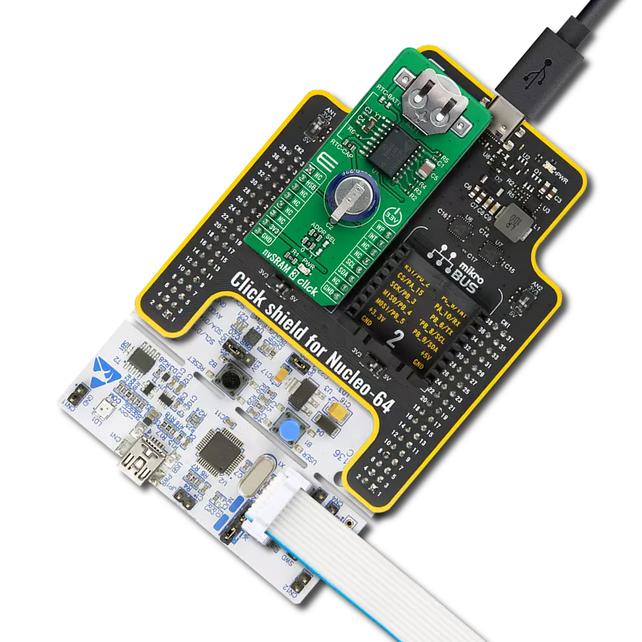
SRAM 3 Click
Dev. board
EasyAVR v7
Compiler
NECTO Studio
MCU
ATmega1284
With our SRAM memory, you can trust in data integrity and fast access for critical operations
A
A
Hardware Overview
How does it work?
SRAM 3 Click is based on the ANV32AA1WDK66, a serial non-volatile SRAM with double memory architecture and SPI serial interface organized as 128k words of 8 bits each from Anvo-System Dresden. This memory has a silicon-oxide-nitride-oxide-silicon (SONOS) flash storage element included with each memory cell. In the case of an unforeseeable operating voltage drop below a defined value, the SONOS technology enables non-volatile data storage in less than 15ms. An integrated Power Down functionality of the SRAM 3 Click with a standby current of less than 1µA ensures low power consumption, with recovery time from Power-Down Mode typically of 60µs. This ANV32AA1WDK66 possesses unique safety features, such as Checksum Protected Memory Accesses (Secure READ and Secure WRITE instructions) and Time Monitoring that ensures a
high degree of reliability of this Click board™. Corrupt data cannot overwrite existing memory content; even valid data would not overwrite on a corrupted address. The SRAM 3 Click also provides some distinctive advantages of SRAMs, such as fast access times and unlimited write/read endurance. SRAM 3 Click incorporates an additional IC, the TXB0108PWR, an 8-bit bidirectional voltage level translator from Texas Instruments. This allows the Click board™ to be used with a much more extensive range of MCUs. At the same time, the TXB0108PWR protects the ANV32AA1WDK66 from the Electrostatic Discharges (ESD) up to ±15 kV, making SRAM 3 Click a very reliable embedded storage solution. The ANV32AA1WDK66 communicates with MCU using the standard SPI serial interface that supports modes 0 and 3 with a maximum
frequency of 66 MHz. It also possesses an additional HOLD function routed at the PWM pin of the mikroBUS™ socket labeled as HLD. This pin is used with the CS pin to select the device. When the device is selected, and a serial sequence is underway, an HLD pin can pause the serial communication with the host device without resetting the serial sequence. This Click board™ can operate with either 3.3V or 5V logic voltage levels selected via the VCC SEL jumper. This way, both 3.3V and 5V capable MCUs can use the communication lines properly. Also, this Click board™ comes equipped with a library containing easy-to-use functions and an example code that can be used as a reference for further development.

Features overview
Development board
EasyAVR v7 is the seventh generation of AVR development boards specially designed for the needs of rapid development of embedded applications. It supports a wide range of 16-bit AVR microcontrollers from Microchip and has a broad set of unique functions, such as a powerful onboard mikroProg programmer and In-Circuit debugger over USB. The development board is well organized and designed so that the end-user has all the necessary elements in one place, such as switches, buttons, indicators, connectors, and others. With four different connectors for each port, EasyAVR v7 allows you to connect accessory boards, sensors, and custom electronics more
efficiently than ever. Each part of the EasyAVR v7 development board contains the components necessary for the most efficient operation of the same board. An integrated mikroProg, a fast USB 2.0 programmer with mikroICD hardware In-Circuit Debugger, offers many valuable programming/debugging options and seamless integration with the Mikroe software environment. Besides it also includes a clean and regulated power supply block for the development board. It can use a wide range of external power sources, including an external 12V power supply, 7-12V AC or 9-15V DC via DC connector/screw terminals, and a power source via the USB Type-B (USB-B)
connector. Communication options such as USB-UART and RS-232 are also included, alongside the well-established mikroBUS™ standard, three display options (7-segment, graphical, and character-based LCD), and several different DIP sockets which cover a wide range of 16-bit AVR MCUs. EasyAVR v7 is an integral part of the Mikroe ecosystem for rapid development. Natively supported by Mikroe software tools, it covers many aspects of prototyping and development thanks to a considerable number of different Click boards™ (over a thousand boards), the number of which is growing every day.

Microcontroller Overview
MCU Card / MCU
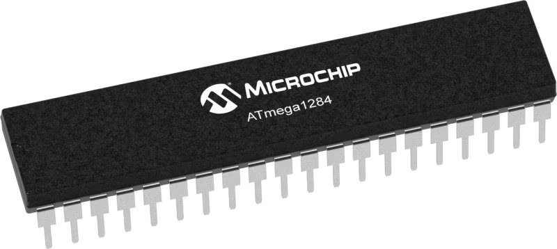
Architecture
AVR
MCU Memory (KB)
128
Silicon Vendor
Microchip
Pin count
40
RAM (Bytes)
16384
Used MCU Pins
mikroBUS™ mapper
Take a closer look
Click board™ Schematic

Step by step
Project assembly

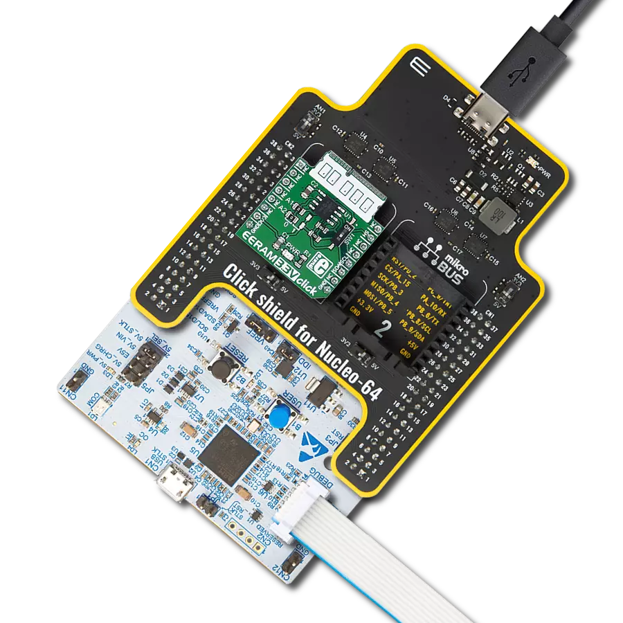
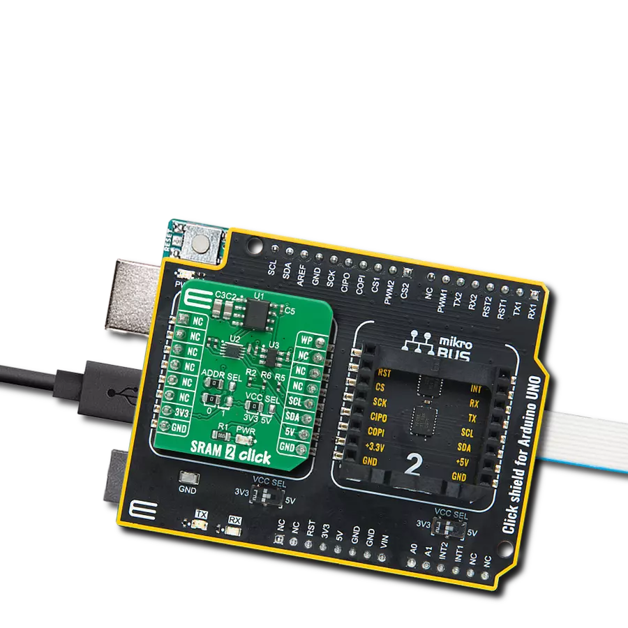
Start by selecting your development board and Click board™. Begin with the EasyAVR v7 as your development board.


Track your results in real time
Application Output
1. Application Output - In Debug mode, the 'Application Output' window enables real-time data monitoring, offering direct insight into execution results. Ensure proper data display by configuring the environment correctly using the provided tutorial.

2. UART Terminal - Use the UART Terminal to monitor data transmission via a USB to UART converter, allowing direct communication between the Click board™ and your development system. Configure the baud rate and other serial settings according to your project's requirements to ensure proper functionality. For step-by-step setup instructions, refer to the provided tutorial.

3. Plot Output - The Plot feature offers a powerful way to visualize real-time sensor data, enabling trend analysis, debugging, and comparison of multiple data points. To set it up correctly, follow the provided tutorial, which includes a step-by-step example of using the Plot feature to display Click board™ readings. To use the Plot feature in your code, use the function: plot(*insert_graph_name*, variable_name);. This is a general format, and it is up to the user to replace 'insert_graph_name' with the actual graph name and 'variable_name' with the parameter to be displayed.

Software Support
Library Description
This library contains API for SRAM 3 Click driver.
Key functions:
sram3_enable_write- This function is for enabling writing to memory, status register or user serial.sram3_disable_write- Function for disabling writing to memory, status register or user serial.sram3_protect_memory- Function which secures part of memory from writing.
Open Source
Code example
The complete application code and a ready-to-use project are available through the NECTO Studio Package Manager for direct installation in the NECTO Studio. The application code can also be found on the MIKROE GitHub account.
/*!
 * @file main.c
 * @brief SRAM3 Click example
 *
 * # Description
 * This is an example that shows the use of SRAM memory, using SRAM 3 Click. SRAM 3 Click is based on ANV32AA1W,
 * and ANV32AA1W is a 1Mb serial SRAM with a non-volatile SONOS storage element included with each memory cell,
 * organized as 128k words of 8 bits each. The devices are accessed by a high speed SPI-compatible bus.
 * Specifically in this example, we used the high-speed SPI communication characteristics to write data to a specific
 * registration address and read it.
 *
 * The demo application is composed of two sections :
 *
 * ## Application Init
 * Initialization SPI module, logger initalization and Click initialization.
 *
 * ## Application Task
 * First, we write the data to the registry address 0x00, and then we read the data from 0x00 address.
 *
 * @author Jelena Milosavljevic
 *
 */

#include "board.h"
#include "log.h"
#include "sram3.h"

static sram3_t sram3;
static log_t logger;
uint8_t buf[10] = { 'M','i','k','r','o','E', 0 };

void application_init ( void ) {
    log_cfg_t log_cfg;         /**< Logger config object. */
    sram3_cfg_t sram3_cfg;     /**< Click config object. */

    /**
     * Logger initialization.
     * Default baud rate: 115200
     * Default log level: LOG_LEVEL_DEBUG
     * @note If USB_UART_RX and USB_UART_TX
     * are defined as HAL_PIN_NC, you will
     * need to define them manually for log to work.
     * See @b LOG_MAP_USB_UART macro definition for detailed explanation.
     */
    LOG_MAP_USB_UART( log_cfg );
    log_init( &logger, &log_cfg );
    log_info( &logger, " Application Init " );

    // Click initialization.
    sram3_cfg_setup( &sram3_cfg );
    SRAM3_MAP_MIKROBUS( sram3_cfg, MIKROBUS_1 );
    err_t init_flag  = sram3_init( &sram3, &sram3_cfg );
    if ( SPI_MASTER_ERROR == init_flag ) {
        log_error( &logger, " Application Init Error. " );
        log_info( &logger, " Please, run program again... " );
        for ( ; ; );
    }

    log_info( &logger, " Application Task " );
    sram3_release_hold( &sram3 );
    Delay_ms ( 100 );
}

void application_task ( void ) {
    char buff_out[ 10 ] = { 0 };

    log_printf( &logger, "Writing [ %s ] to memory...\r\n", buf );
    sram3_enable_write( &sram3 );
    sram3_write( &sram3, 0x00, &buf[0], 6 );

    Delay_ms ( 100 );
    sram3_read( &sram3, 0x00, &buff_out[0], 6 );
    Delay_ms ( 100 );
    log_printf( &logger, "Data read from memory: %s \r\n", buff_out );
    log_printf( &logger, "---------------------------------------------\r\n" );

    Delay_ms ( 1000 );
    Delay_ms ( 1000 );
}

int main ( void )
{
    /* Do not remove this line or clock might not be set correctly. */
    #ifdef PREINIT_SUPPORTED
    preinit();
    #endif

    application_init( );

    for ( ; ; )
    {
        application_task( );
    }

    return 0;
}

// ------------------------------------------------------------------------ END