Transform your projects into hubs of efficiency with AP33771 and ATmega644
USB-C sink – Uniting speed, power, and style!

Published Nov 13, 2023
Click board™
USB-C Sink 3 Click
Dev. board
EasyAVR v7
Compiler
NECTO Studio
MCU
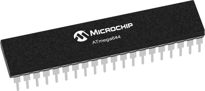
ATmega644
Revolutionize your project experience with our USB-C sink solution, paving the way for faster data transfers and smarter power management.
A
A
Hardware Overview
How does it work?
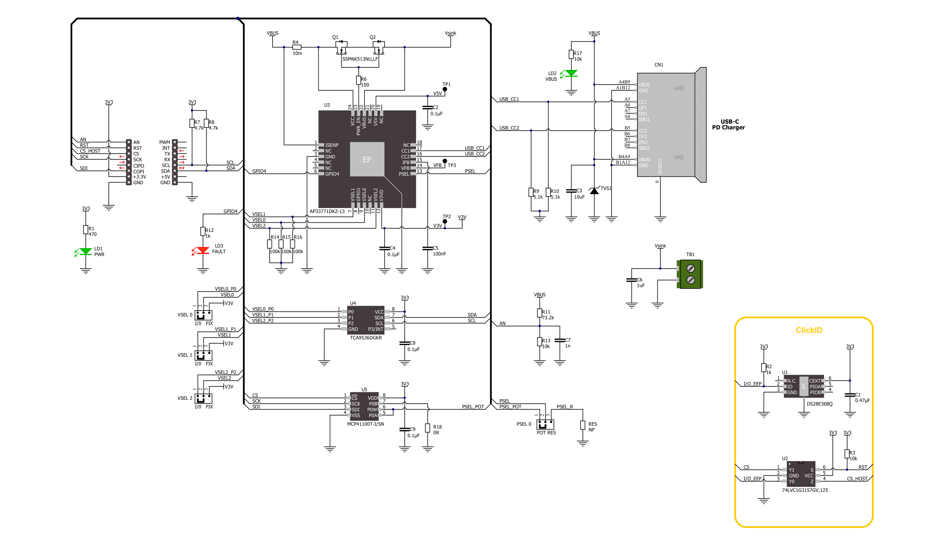
USB-C Sink 3 Click is based on the AP33771, a high-performance USB PD sink controller from Diodes Incorporated. It supports up to eight voltage selections alongside ten different power range selections. In addition to selected voltages, both fixed PDO and PPS APDO in the PD source adapter are supported in the AP33771 search algorithm. The PD controller supports OVP with auto-restart, one-time programming (OTP) ROM for main firmware, and power capability selection. The onboard FAULT LED serves as a visual presentation of the negotiation mismatch. USB-C Sink 3 Click is equipped with a VSINK, an external power supply terminal that comes with a pair of MOSFETs, according to the AP33771’s driver for N-MOS VBUS power switch support. The PD controller can control the external NMOS switch ON or OFF. The USB-C connector acts as a PD-IN discharge path terminal with a USB Type-C configuration channels 1 and 2. The presence of the power supply on the USB C is indicated over
the VBUS LED. The USB-C Sink 3 Click comes with a VSEL three 2-position jumpers labeled 0, 1, and 2 to select the desired target voltage. I/O and FIX(ed) sides allow you to choose between hardware and software target voltage selection in eight positions and a target voltage range from 5V up to 17.2V. The VSEL is set to I/O by default, where you can set logic states to the three IO pins over the TCA9536, a remote 4-bit I2C, and SMBus I/O expander with configuration registers from Texas Instruments. The table of the combination of the positions and the resulting target voltages is printed at the bottom of the Click board™. You can use fixed jumper positions by setting the jumpers as you like, where I/O acts as a 0 and 3V3 as a 1 position. The 5V and 3.3V LDO voltage output can be measured over the V5V and V3V pads and voltage feedback over the VFB pad. To select the desired power, there is the MCP41100T, a digital potentiometer with an SPI interface from Microchip. Selecting the corresponding resistance
value on the digital potentiometer allows you to choose one of the current capabilities ranging from 12W to 100W. The table with the expected resistance and the resulting current is printed at the bottom of the Click board™. In addition, you can solder a standard resistor by soldering it on RES resistor pads. For that purpose, you should set the PSEL jumper to a RES position, as it is set to a POT position by default. USB-C Sink 3 Click uses a standard 2-Wire I2C interface of the MCP41100T to communicate with the host MCU. One of the main features of the USB-C Sink 3 Click is the ability to track the VBUS voltage over the AN pin of the mikroBUS™ socket. This Click board™ can be operated only with a 3.3V logic voltage level. The board must perform appropriate logic voltage level conversion before using MCUs with different logic levels. Also, it comes equipped with a library containing functions and an example code that can be used as a reference for further development.

Features overview
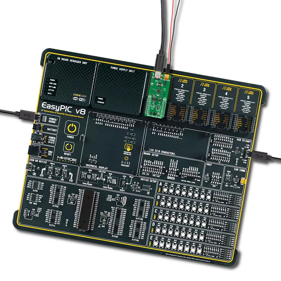
Development board
EasyAVR v7 is the seventh generation of AVR development boards specially designed for the needs of rapid development of embedded applications. It supports a wide range of 16-bit AVR microcontrollers from Microchip and has a broad set of unique functions, such as a powerful onboard mikroProg programmer and In-Circuit debugger over USB. The development board is well organized and designed so that the end-user has all the necessary elements in one place, such as switches, buttons, indicators, connectors, and others. With four different connectors for each port, EasyAVR v7 allows you to connect accessory boards, sensors, and custom electronics more
efficiently than ever. Each part of the EasyAVR v7 development board contains the components necessary for the most efficient operation of the same board. An integrated mikroProg, a fast USB 2.0 programmer with mikroICD hardware In-Circuit Debugger, offers many valuable programming/debugging options and seamless integration with the Mikroe software environment. Besides it also includes a clean and regulated power supply block for the development board. It can use a wide range of external power sources, including an external 12V power supply, 7-12V AC or 9-15V DC via DC connector/screw terminals, and a power source via the USB Type-B (USB-B)
connector. Communication options such as USB-UART and RS-232 are also included, alongside the well-established mikroBUS™ standard, three display options (7-segment, graphical, and character-based LCD), and several different DIP sockets which cover a wide range of 16-bit AVR MCUs. EasyAVR v7 is an integral part of the Mikroe ecosystem for rapid development. Natively supported by Mikroe software tools, it covers many aspects of prototyping and development thanks to a considerable number of different Click boards™ (over a thousand boards), the number of which is growing every day.

Microcontroller Overview
MCU Card / MCU
Architecture
AVR
MCU Memory (KB)
64
Silicon Vendor
Microchip
Pin count
40
RAM (Bytes)
4096
Used MCU Pins
mikroBUS™ mapper
Take a closer look
Click board™ Schematic
Step by step
Project assembly

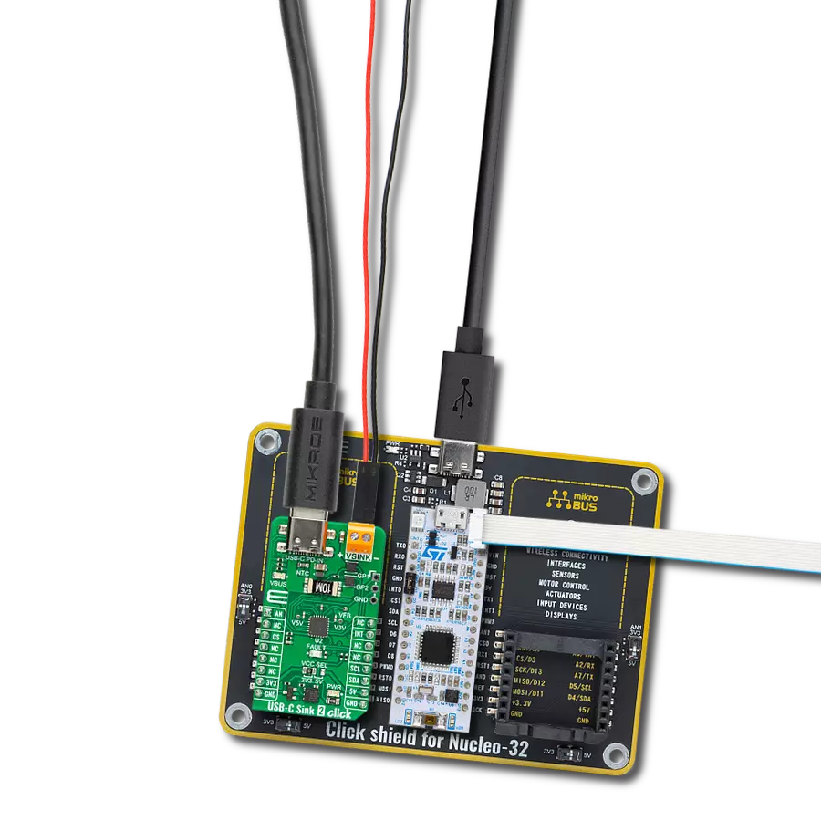
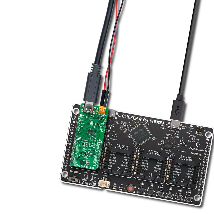
Start by selecting your development board and Click board™. Begin with the EasyAVR v7 as your development board.


Software Support
Library Description
This library contains API for USB-C Sink 3 Click driver.
Key functions:
usbcsink3_set_voltage- USB-C Sink 3 set the voltage function.usbcsink3_set_power- USB-C Sink 3 set the power function.usbcsink3_get_vbus- USB-C Sink 3 get VBUS function.
Open Source
Code example
The complete application code and a ready-to-use project are available through the NECTO Studio Package Manager for direct installation in the NECTO Studio. The application code can also be found on the MIKROE GitHub account.
/*!
 * @file main.c
 * @brief USB-C Sink 3 Click example
 *
 * # Description
 * This example demonstrates the use of USB-C Sink 3 Click board™
 * by setting DC power requests and control for Type-C connector-equipped devices (TCD).
 *
 * The demo application is composed of two sections :
 *
 * ## Application Init
 * Initializes SPI, I2C and ADC modules and log UART.
 * After driver initialization the app set default settings:
 * Voltage Selection: 5 [V] and Power: 15.0 [W].
 *
 * ## Application Task
 * In this example, the app configures Power Data Objects (PDO)
 * highest priority profile and requests power from a standard USB PD source adapter.
 * It interprets power input requirements (voltage/current and maximum power) from the TCD.
 * The example uses two configurations:
 *  - Voltage 5 [V] and Power 15.0 [W]
 *  - Voltage 9 [V] and Power 18.0 [W]
 * Results are being sent to the Usart Terminal where you can track their changes.
 *
 * @note
 * FAULT LED flickering notified of the system status:
 *  - Charging: Breathing light (2 sec dimming), 1 cycle is 4 sec.
 *  - Fully charged: Continuously lit Charging current < 500mA.
 *  - Mismatch: 1s flicker Voltage or power mismatch. Non-PD power source, 1 cycle is 2sec.
 *  - Fault: 300ms flicker OVP, 1 cycle is 600ms.
 *
 * @author Nenad Filipovic
 *
 */

#include "board.h"
#include "log.h"
#include "usbcsink3.h"

static usbcsink3_t usbcsink3;
static log_t logger;

void application_init ( void )
{
    log_cfg_t log_cfg;  /**< Logger config object. */
    usbcsink3_cfg_t usbcsink3_cfg;  /**< Click config object. */

    /**
     * Logger initialization.
     * Default baud rate: 115200
     * Default log level: LOG_LEVEL_DEBUG
     * @note If USB_UART_RX and USB_UART_TX
     * are defined as HAL_PIN_NC, you will
     * need to define them manually for log to work.
     * See @b LOG_MAP_USB_UART macro definition for detailed explanation.
     */
    LOG_MAP_USB_UART( log_cfg );
    log_init( &logger, &log_cfg );
    log_info( &logger, " Application Init " );

    // Click initialization.
    usbcsink3_cfg_setup( &usbcsink3_cfg );
    USBCSINK3_MAP_MIKROBUS( usbcsink3_cfg, MIKROBUS_1 );
    err_t init_flag = usbcsink3_init( &usbcsink3, &usbcsink3_cfg );
    if ( ( I2C_MASTER_ERROR == init_flag ) || ( SPI_MASTER_ERROR == init_flag ) )
    {
        log_error( &logger, " Communication init." );
        for ( ; ; );
    }
    Delay_ms ( 100 );

    if ( USBCSINK3_ERROR == usbcsink3_default_cfg ( &usbcsink3 ) )
    {
        log_error( &logger, " Default configuration." );
        for ( ; ; );
    }
    Delay_ms ( 100 );

    log_info( &logger, " Application Task " );
    log_printf( &logger, " ------------------------\r\n" );
    Delay_ms ( 1000 );
}

void application_task ( void )
{
    static float voltage = 0.0;
    if ( ( USBCSINK3_OK == usbcsink3_set_voltage( &usbcsink3, USBCSINK3_VTG_SEL_5V ) ) &&
         ( USBCSINK3_OK == usbcsink3_set_power( &usbcsink3, USBCSINK3_PWR_SEL_15W ) ) )
    {
        log_printf( &logger, " Output:\r\nVoltage: 5.0 [V]\r\nPower: 15.0 [W]\r\n" );
        log_printf( &logger, " - - - - - -  - - - - - -\r\n" );
        Delay_ms ( 1000 );
        usbcsink3_get_vbus ( &usbcsink3, &voltage );
        log_printf( &logger, " VBUS : %.1f [V]\r\n", voltage );
        log_printf( &logger, " ------------------------\r\n" );
        Delay_ms ( 1000 );
        Delay_ms ( 1000 );
        Delay_ms ( 1000 );
        Delay_ms ( 1000 );
        Delay_ms ( 1000 );
    }

    if ( ( USBCSINK3_OK == usbcsink3_set_voltage( &usbcsink3, USBCSINK3_VTG_SEL_9V ) ) &&
         ( USBCSINK3_OK == usbcsink3_set_power( &usbcsink3, USBCSINK3_PWR_SEL_18W ) ) )
    {
        log_printf( &logger, " Output:\r\nVoltage: 9.0 [V]\r\nPower: 18.0 [W]\r\n" );
        log_printf( &logger, " - - - - - -  - - - - - -\r\n" );
        Delay_ms ( 1000 );
        usbcsink3_get_vbus ( &usbcsink3, &voltage );
        log_printf( &logger, " VBUS : %.1f [V]\r\n", voltage );
        log_printf( &logger, " ------------------------\r\n" );
        Delay_ms ( 1000 );
        Delay_ms ( 1000 );
        Delay_ms ( 1000 );
        Delay_ms ( 1000 );
        Delay_ms ( 1000 );
    }
}

int main ( void )
{
    /* Do not remove this line or clock might not be set correctly. */
    #ifdef PREINIT_SUPPORTED
    preinit();
    #endif

    application_init( );

    for ( ; ; )
    {
        application_task( );
    }

    return 0;
}

// ------------------------------------------------------------------------ END