Deliver faster and more efficient data transfer with MICRF230 and PIC32MZ1024EFH064
Stay in control, stay connected

Published Nov 07, 2023
Click board™
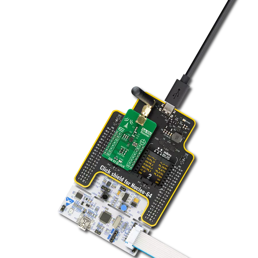
OOK RX Click
Dev. board
PIC32MZ clicker
Compiler
NECTO Studio
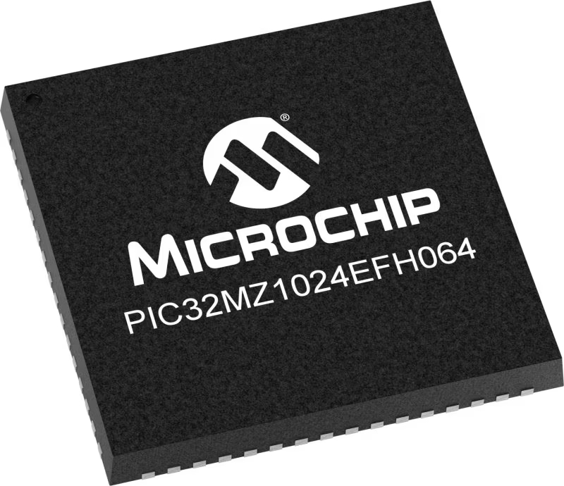
MCU
PIC32MZ1024EFH064
Our 433MHz wireless receiver puts you in control by ensuring a strong, uninterrupted link between your devices, keeping you connected no matter the distance
A
A
Hardware Overview
How does it work?
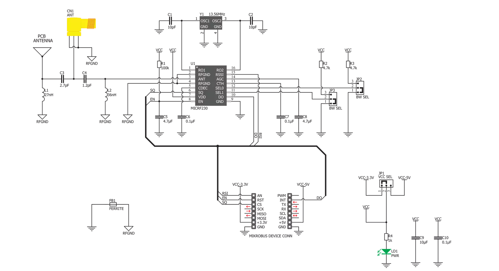
OOK RX Click is based on the MICRF230, a 400MHz to 450MHz ASK/OOK receiver with RSSI and squelch, from Microchip. The working principle of this device is based on decoding of information embedded in a radio signal. The ASK/OOK modulation is a way to encode information and assemble it into radio signals which can be transmitted and received wirelessly. Generally, ASK is an abbreviate for the Amplitude Shift Key modulation, which is realized by shifting the amplitude of the signal, depending on the number that is going to be transmitted. For example, if the transmitted number is 1, the transmitted signal amplitude would be equal to the carrier signal amplitude, if the transmitted number is 2, the transmitted signal amplitude is as twice as the carrier signal amplitude and so on. The ASK method of modulation allows not only the binary communication, as more than two signal amplitudes can be detected by the receiver. However, this method is very susceptible to noise and interferences. To overcome this problem, an OOK modulation method was introduced. The OOK modulation is very similar to the ASK, but it is of a binary type. OOK is an abbreviate for the Off-On Key, which perfectly describes this type of modulation. The presence of the carrier signal is recognized as the logical 1, while the absence of a carrier signal is recognized as the logical 0. This method is more immune to noise and interferences than the ASK modulation, and it allows for greater communication distance to be achieved. Signal demodulation starts with the RF signal being received and amplified by the low noise amplifier at the RF input. This signal is
additionally processed by the internal mixers, filters and frequency synthesizers, and the processed intermediate frequency (IF) signal of about 330kHz is generated. This signal is passed to the decoding section. Decoder removes the carrier signal from the IF and filters the remaining baseband signal. This is done by a low pass filter with a user selectable bandwidth. The bandwidth choice is very important as it provides the optimal bit error rate (BER) for a specific data rate. Depending on the transmitted information data rate, users can select the bandwidth of the low pass filter, by moving the onboard SMD jumpers, labeled as BW SEL. These jumpers are used to set SEL0 and SEL1 pins of the IC to the proper logic levels, as you can see from the table given below. Before the communication is attempted, the preamble burst should be received first. The preamble burst allows calibration to the receiving signal. When resuming from the Shutdown mode, the preamble should be long enough to allow the receiver to be fully awake and ready to receive data. The integrated squelch function is used to limit the activity on the DO (data output) pin. This is particularly useful if the DO is used for an interrupt generation, as the squelch function will suppress any activity unless valid communication bits are detected. When the SQ pin is set to a logic LOW level, the squelch functionality is enabled, reducing random activity (noise) on the DO pin when there is no RF input signal. The SQ pin is pulled to a logic HIGH level internally, so it is disabled if the pin is left afloat. This pin is routed to the CS pin of the mikroBUS™. Power consumption can be reduced if the device is put into the
Shutdown mode. When EN pin is pulled high, the internal logic of the MICRF230 IC is activated. The EN pin is internally pulled LOW so that the device starts in the Shutdown mode when this pin is left afloat. The onboard capacitor ensures a proper power-up cycle since it will generate a small delay before the EN pin is pulled to a logic HIGH level, giving time to the power supply voltage to stabilize. The EN pin is routed to the mikroBUS™ RST pin. OOK RX click has an RSSI (received signal strength indicator) output pin, used to directly measure the voltage level on the AGC (automatic gain compensation) section. The AGC is an integrated circuit section that provides a constant amplitude of the low pass filtered baseband signal. The voltage level on this pin determines the amplification of the AGC section. Since this level is not directly readable, an inverted, buffered version of the voltage is present on the RSSI pin, which can be directly used to determine the signal strength - which is inversely proportional to the signal amplification. The RSSI output pin has an impedance of 200Ω and it is routed to the AN pin of the mikroBUS™. OOK RX click can work both with an integrated PCB trace antenna or a 433MHz external antenna, which can be attached to the onboard SMA connector of the click board, for improved range and received signal strength. Both 3.3V and 5V operation is supported by this click board™. By moving the SMD jumper labeled as the VCC SEL, it is possible to select the operating voltage, so that both 3.3V and 5V capable MCUs can work with the OOK RX click board.

Features overview
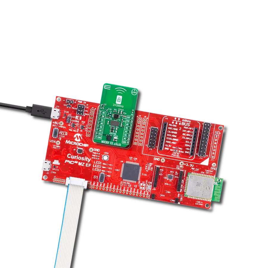
Development board
PIC32MZ Clicker is a compact starter development board that brings the flexibility of add-on Click boards™ to your favorite microcontroller, making it a perfect starter kit for implementing your ideas. It comes with an onboard 32-bit PIC32MZ microcontroller with FPU from Microchip, a USB connector, LED indicators, buttons, a mikroProg connector, and a header for interfacing with external electronics. Thanks to its compact design with clear and easy-recognizable silkscreen markings, it provides a fluid and immersive working experience, allowing access anywhere and under
any circumstances. Each part of the PIC32MZ Clicker development kit contains the components necessary for the most efficient operation of the same board. In addition to the possibility of choosing the PIC32MZ Clicker programming method, using USB HID mikroBootloader, or through an external mikroProg connector for PIC, dsPIC, or PIC32 programmer, the Clicker board also includes a clean and regulated power supply module for the development kit. The USB Micro-B connection can provide up to 500mA of current, which is more than enough to operate all onboard
and additional modules. All communication methods that mikroBUS™ itself supports are on this board, including the well-established mikroBUS™ socket, reset button, and several buttons and LED indicators. PIC32MZ Clicker is an integral part of the Mikroe ecosystem, allowing you to create a new application in minutes. Natively supported by Mikroe software tools, it covers many aspects of prototyping thanks to a considerable number of different Click boards™ (over a thousand boards), the number of which is growing every day.

Microcontroller Overview
MCU Card / MCU
Architecture
PIC32
MCU Memory (KB)
1024
Silicon Vendor
Microchip
Pin count
64
RAM (Bytes)
524288
You complete me!
Accessories
Right angle 433MHz rubber antenna boasts a frequency range of 433MHz, ensuring optimal performance within this spectrum. With a 50Ohm impedance, it facilitates efficient signal transmission. The antenna's vertical polarization enhances signal reception in a specific orientation. Featuring a 1.5dB gain, it can improve signal strength to some extent. The antenna can handle a maximum input power of 50W, making it suitable for various applications. Its compact 50mm length minimizes spatial requirements. Equipped with an SMA male connector, it easily interfaces with compatible devices. This antenna is an adaptable solution for wireless communication needs, particularly when vertical polarization is crucial.

Used MCU Pins
mikroBUS™ mapper
Take a closer look
Click board™ Schematic
Step by step
Project assembly

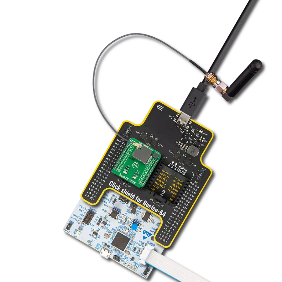
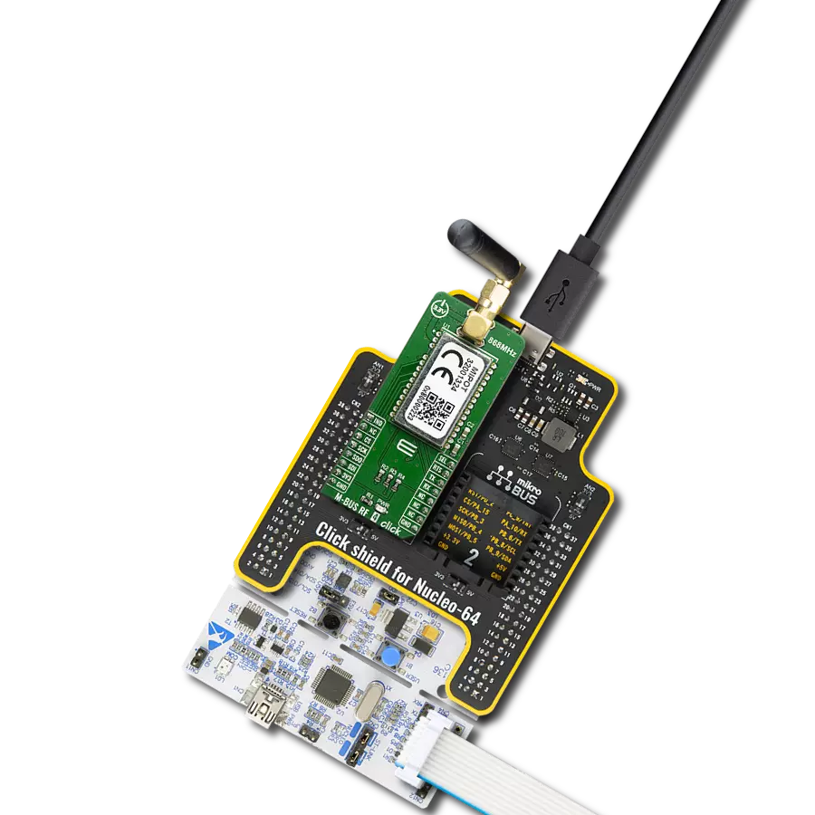
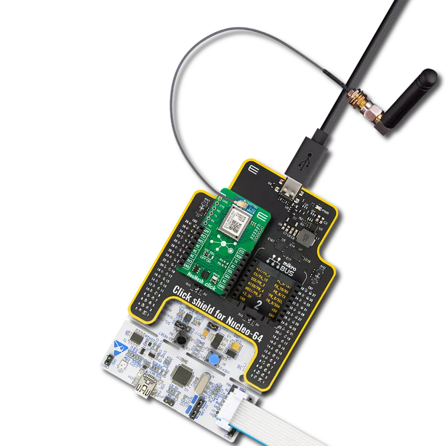
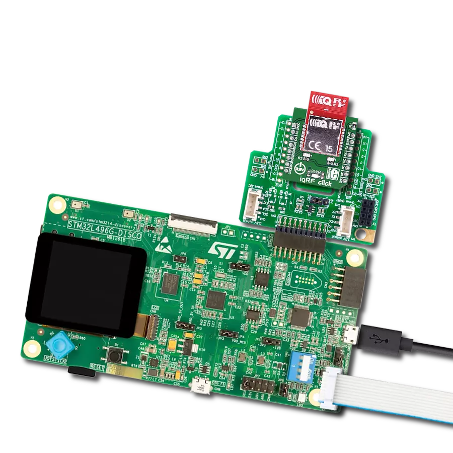
Start by selecting your development board and Click board™. Begin with the PIC32MZ clicker as your development board.


Track your results in real time
Application Output
1. Application Output - In Debug mode, the 'Application Output' window enables real-time data monitoring, offering direct insight into execution results. Ensure proper data display by configuring the environment correctly using the provided tutorial.

2. UART Terminal - Use the UART Terminal to monitor data transmission via a USB to UART converter, allowing direct communication between the Click board™ and your development system. Configure the baud rate and other serial settings according to your project's requirements to ensure proper functionality. For step-by-step setup instructions, refer to the provided tutorial.

3. Plot Output - The Plot feature offers a powerful way to visualize real-time sensor data, enabling trend analysis, debugging, and comparison of multiple data points. To set it up correctly, follow the provided tutorial, which includes a step-by-step example of using the Plot feature to display Click board™ readings. To use the Plot feature in your code, use the function: plot(*insert_graph_name*, variable_name);. This is a general format, and it is up to the user to replace 'insert_graph_name' with the actual graph name and 'variable_name' with the parameter to be displayed.

Software Support
Library Description
This library contains API for OOK RX Click driver.
Key functions:
ookrx_receive_data- This function receives data in the OOK communication.ookrx_read_do_pin- This function reads the od pin digital input.ookrx_read_rsi_pin- This function reads the rsi pin digital input.
Open Source
Code example
The complete application code and a ready-to-use project are available through the NECTO Studio Package Manager for direct installation in the NECTO Studio. The application code can also be found on the MIKROE GitHub account.
/*!
 * @file main.c
 * @brief OOK RX Click Example.
 *
 * # Description
 * This example demonstrates the use of OOK RX Click board by reading and parsing
 * packet messages received from the transmitter.
 *
 * The demo application is composed of two sections :
 *
 * ## Application Init
 * Initializes the driver and enables the device and squelch mode.
 *
 * ## Application Task
 * Waits for a data ready indication, then reads all packet data, verifies the CRC
 * bytes in a packet, and displays its data as well as the RSSI value on the USB UART.
 *
 * @note
 * The OOK TX Click board is a compatible transmitter for the OOK RX Click.
 * Here are a few steps for troubleshooting if you are experiencing issues running
 * this example:
 *  - Check the MCU clock configuration, use an external oscillator instead of the MCU's
 * internal one for better accuracy on manchester data rate delay.
 *  - Measure the actual data rate on the data line and adjust the OOKRX_MAN_BIT_LEN_US
 * value accordingly.
 *
 * @author Stefan Filipovic
 *
 */

#include "board.h"
#include "log.h"
#include "ookrx.h"

#define OOKRX_PREAMBLE      0x5AA5  /**< Packet preamble word. */

static ookrx_t ookrx;       /**< OOK RX Click driver object. */
static log_t logger;        /**< Logger object. */
static uint8_t packet_buf[ OOKRX_MAX_DATA_LEN + 5 ] = { 0 };  /**< Packet buffer. */

/**
 * @brief OOK RX wait ready function.
 * @details This function waits for all training bytes to arrive which indicates data ready.
 * @param[in] ctx : Click context object.
 * See #ookrx_t object definition for detailed explanation.
 * @return None.
 * @note None.
 */
static void ookrx_wait_ready ( ookrx_t *ctx );

/**
 * @brief OOK RX read packet function.
 * @details This function reads data packet and stores it in a packet_buf only if
 * the OOKRX_PREAMBLE bytes are received successfully.
 * @param[in] ctx : Click context object.
 * See #ookrx_t object definition for detailed explanation.
 * @return Number of data bytes stored in a packet_buf.
 * @note The expected packet format is as follows (MSB first, manchester IEEE 802.3):
 * TRAINING_BYTES (at least two bytes of 0xAA), PREABMLE, LEN, DATA_IN, CRC16 (calculated
 * from whole packet excluding training bytes). Training bytes are excluded from packet_buf.
 * This function must be called immediately after calling ookrx_wait_ready.
 */
static uint8_t ookrx_read_packet ( ookrx_t *ctx );

/**
 * @brief Reflect bits.
 * @details This function reflects a desired number of bits in data.
 * @return Reflected data.
 * @note None.
 */
static uint16_t ookrx_reflect_bits( uint16_t data_in, uint8_t len );

/**
 * @brief CRC-16/MAXIM calculation for CRC16 function.
 * @details This function calculates CRC16 with parameteres:
 * @li @c  Width 16 bit
 * @li @c  Polynomial 0x8005 ( x16 + x15 + x2 + x0 )
 * @li @c  Initialization 0x0000
 * @li @c  Reflect input True
 * @li @c  Reflect output True
 * @li @c  Final Xor 0xFFFF
 * @li @c  Example { 69, 00 } - 0xAFD1
 * @param[in] data_buf : Array of bytes to calculate crc from.
 * @param[in] len : Number of bytes to calculate crc from.
 * @return Calculated CRC.
 * @note None.
 */
static uint16_t ookrx_calculate_crc16 ( uint8_t *data_buf, uint16_t len );

void application_init ( void )
{
    log_cfg_t log_cfg;      /**< Logger config object. */
    ookrx_cfg_t ookrx_cfg;  /**< Click config object. */

    /**
     * Logger initialization.
     * Default baud rate: 115200
     * Default log level: LOG_LEVEL_DEBUG
     * @note If USB_UART_RX and USB_UART_TX
     * are defined as HAL_PIN_NC, you will
     * need to define them manually for log to work.
     * See @b LOG_MAP_USB_UART macro definition for detailed explanation.
     */
    LOG_MAP_USB_UART( log_cfg );
    log_init( &logger, &log_cfg );
    log_info( &logger, " Application Init " );

    // Click initialization.
    ookrx_cfg_setup( &ookrx_cfg );
    OOKRX_MAP_MIKROBUS( ookrx_cfg, MIKROBUS_1 );
    if ( DIGITAL_OUT_UNSUPPORTED_PIN == ookrx_init( &ookrx, &ookrx_cfg ) )
    {
        log_error( &logger, " Communication init." );
        for ( ; ; );
    }

    ookrx_enable_squelch ( &ookrx );
    ookrx_enable_device ( &ookrx );

    log_info( &logger, " Application Task " );
}

void application_task ( void )
{
    static float rssi_v = 0;
    static uint8_t packet_len = 0;
    static uint8_t msg_cnt = 0;
    static uint16_t crc = 0;

    log_printf( &logger, "\r\n Waiting for data ready...\r\n" );
    ookrx_wait_ready ( &ookrx );
    packet_len = ookrx_read_packet ( &ookrx );
    if ( packet_len )
    {
        ookrx_read_rssi_voltage ( &ookrx, &rssi_v );
        crc = ( ( uint16_t ) packet_buf[ packet_len - 2 ] << 8 ) | packet_buf[ packet_len - 1 ];
        if ( crc == ookrx_calculate_crc16 ( packet_buf, packet_len - 2 ) )
        {
            log_printf( &logger, " Received message: " );
            for ( msg_cnt = 0; msg_cnt < packet_buf[ 2 ]; msg_cnt++ )
            {
                log_printf( &logger, "%c", ( uint16_t ) packet_buf[ msg_cnt + 3 ] );
            }
            log_printf( &logger, "\r\n RSSI: %.1f dBm\r\n", OOKRX_RSSI_V_TO_DBM ( rssi_v ) );
        }
    }
    Delay_ms ( 100 );
}

int main ( void )
{
    /* Do not remove this line or clock might not be set correctly. */
    #ifdef PREINIT_SUPPORTED
    preinit();
    #endif

    application_init( );

    for ( ; ; )
    {
        application_task( );
    }

    return 0;
}

static void ookrx_wait_ready ( ookrx_t *ctx )
{
    uint16_t time_cnt = 0;
    uint16_t training_high_cnt = 0;
    uint16_t training_low_cnt = 0;
    // Loop until at least two 0xAA bytes of training data is detected
    for ( ; ; )
    {
        // Measure time in steps of OOKRX_MAN_BIT_LEN_US / 40 for high signal
        for ( time_cnt = 0; ookrx_get_data_pin ( ctx ); time_cnt++ )
        {
            Delay_us ( OOKRX_MAN_BIT_LEN_US / 40 );
        }
        if ( time_cnt > 30 )
        {
            // Increment training_high_cnt if signal width is at least 75% of OOKRX_MAN_BIT_LEN_US
            training_high_cnt++;
        }
        else
        {
            // Reset counters if any invalid signal is detected
            training_high_cnt = 0;
            training_low_cnt = 0;
        }

        // Measure time in steps of OOKRX_MAN_BIT_LEN_US / 40 for low signal
        for ( time_cnt = 0; ( training_high_cnt > 0 ) && !ookrx_get_data_pin ( ctx ); time_cnt++ )
        {
            Delay_us ( OOKRX_MAN_BIT_LEN_US / 40 );
        }
        if ( time_cnt > 30 )
        {
            // Increment training_low_cnt if signal width is at least 75% of OOKRX_MAN_BIT_LEN_US
            training_low_cnt++;
        }
        else if ( ( training_high_cnt >= 8 ) && ( training_high_cnt == ( training_low_cnt + 1 ) ) )
        {
            // At least two 0xAA bytes are detected ending with shorter low signal, so break the loop here.
            // Waiting for 12.5% of OOKRX_MAN_BIT_LEN_US as an offset for packet reading.
            Delay_us ( OOKRX_MAN_BIT_LEN_US / 8 );
            break;
        }
    }
}

static uint8_t ookrx_read_packet ( ookrx_t *ctx )
{
    uint8_t byte_cnt = 0;
    uint8_t bit_cnt = 0;
    // Loop until all data bytes are received or a bad PREAMBLE word is detected
    for ( ; ; )
    {
        if ( !ookrx_get_data_pin ( ctx ) )
        {
            // Store data in packet_buf in manchester IEEE 802.3 format, MSB first
            packet_buf[ byte_cnt ] |= ( 0x80 >> bit_cnt );
        }

        if ( 8 == ++bit_cnt )
        {
            // Reset bit counter and increment byte counter if 8 bits are received
            bit_cnt = 0;
            byte_cnt++;
        }

        if ( 2 == byte_cnt )
        {
            // Two bytes are received, check PREAMBLE word
            if ( OOKRX_PREAMBLE != ( ( ( uint16_t ) packet_buf[ 0 ] << 8 ) | packet_buf[ 1 ] ) )
            {
                byte_cnt = 0;
                break;
            }
        }
        else if ( ( packet_buf[ 2 ] + 5 ) == byte_cnt )
        {
            // Break the loop if all packet data are received (PREAMBLE + DATA_LEN + DATA + CRC)
            break;
        }

        // Move to the next manchester clock high state by delaying for OOKRX_MAN_BIT_LEN_US
        Delay_us ( OOKRX_MAN_BIT_LEN_US );
    }
    return byte_cnt;
}

static uint16_t ookrx_reflect_bits( uint16_t data_in, uint8_t len )
{
    uint16_t data_out = 0;
    for ( uint16_t cnt = 0; cnt < len; cnt++ )
    {
        data_out |= ( ( data_in >> cnt ) & 1 ) << ( len - cnt - 1 );
    }
    return data_out;
}

static uint16_t ookrx_calculate_crc16( uint8_t *data_buf, uint16_t len )
{
    uint16_t crc16 = 0x0000;
    for ( uint16_t cnt = 0; cnt < len; cnt++ )
    {
        crc16 ^= ( ookrx_reflect_bits( data_buf[ cnt ], 8 ) << 8 );
        for ( uint8_t bit_cnt = 0; bit_cnt < 8; bit_cnt++ )
        {
            if ( crc16 & 0x8000 )
            {
                crc16 = ( crc16 << 1 ) ^ 0x8005;
            }
            else
            {
                crc16 <<= 1;
            }
        }
    }
    return ookrx_reflect_bits( crc16, 16 ) ^ 0xFFFF;
}

// ------------------------------------------------------------------------ END
Additional Support
Resources
Category:Sub-1 GHz Transceievers