Experience seamless multitasking and quick data processing with 23LC1024 and MK64FN1M0VDC12
Highly reliable nonvolatile memory

Published Oct 26, 2023
Click board™
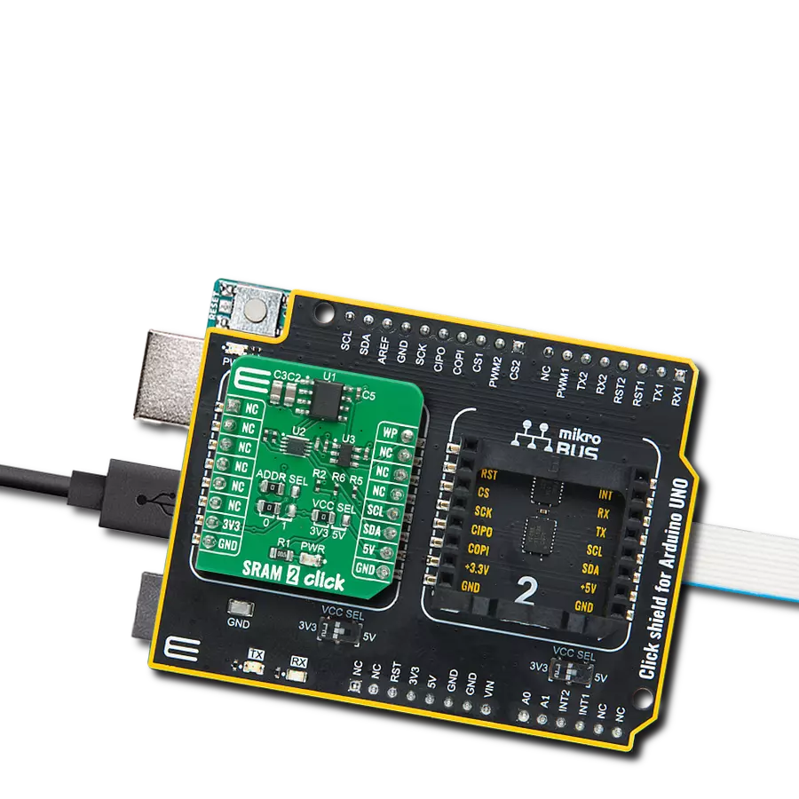
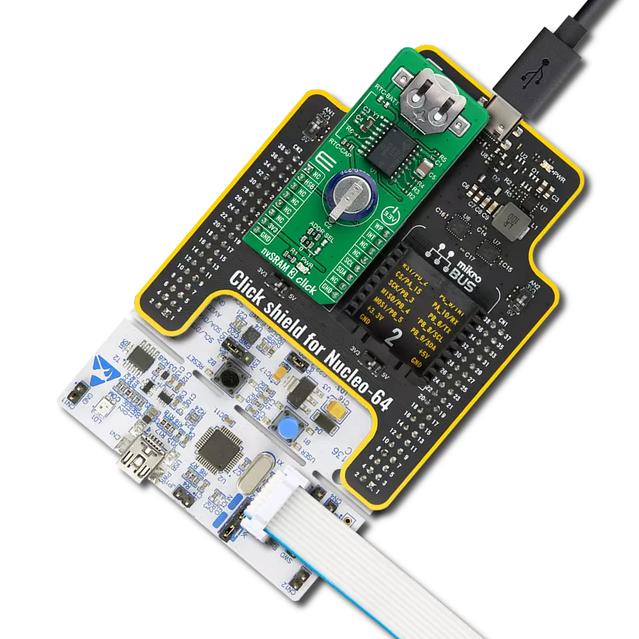
SRAM Click
Dev. board
Clicker 2 for Kinetis
Compiler
NECTO Studio
MCU
MK64FN1M0VDC12
Whether it's in networking, embedded systems, or consumer electronics, SRAM memory solutions drive performance to new heights
A
A
Hardware Overview
How does it work?
SRAM Click is based on the 23LC1024, a highly reliable 1Mbit Serial SRAM designed to interface directly with Microchip's Serial Peripheral Interface (SPI). The 23LC1024 is organized as 128k words of 8 bits each and provides fast access alongside infinite read and write cycles to the memory array. The embedded nonvolatile elements incorporate the CMOS technology, making this Click board™ an ideal choice for secure data storage, creating the world's most reliable nonvolatile memory. The serial SRAM has three modes of operation, byte, page, and sequential, which are chosen by setting bits in the MODE register. In Byte mode, the R/W operations are limited to only one byte,
while in Page mode, R/W operations are limited to within the addressed page. The last Sequential mode allows the entire array to be written to and read from. The 23LC1024 communicates with MCU through a standard SPI interface that enables very high clock speeds up to 20MHz with zero cycle delay read and write cycles. It may also interface with MCUs that do not have a built-in SPI port by using discrete I/O lines programmed properly in firmware to match the SPI protocol. In addition, the 23LC1024 can operate in SDI and SQI modes. In the SDI mode, the SI and SO data lines are bidirectional, allowing the transfer of two bits per clock pulse, while in the SQI mode, two additional
data lines enable the transfer of four bits per clock pulse. The SRAM Click also has an additional HOLD signal, routed to the RST pin of the mikroBUS™ socket labeled as HLD, used to suspend the serial communication without resetting the serial sequence. This Click board™ can operate with both 3.3V and 5V logic voltage levels selected via the PWR SEL jumper. This way, both 3.3V and 5V capable MCUs can use the communication lines properly. Also, this Click board™ comes equipped with a library containing easy-to-use functions and an example code that can be used as a reference for further development.

Features overview
Development board
Clicker 2 for Kinetis is a compact starter development board that brings the flexibility of add-on Click boards™ to your favorite microcontroller, making it a perfect starter kit for implementing your ideas. It comes with an onboard 32-bit ARM Cortex-M4F microcontroller, the MK64FN1M0VDC12 from NXP Semiconductors, two mikroBUS™ sockets for Click board™ connectivity, a USB connector, LED indicators, buttons, a JTAG programmer connector, and two 26-pin headers for interfacing with external electronics. Its compact design with clear and easily recognizable silkscreen markings allows you to build gadgets with unique functionalities and
features quickly. Each part of the Clicker 2 for Kinetis development kit contains the components necessary for the most efficient operation of the same board. In addition to the possibility of choosing the Clicker 2 for Kinetis programming method, using a USB HID mikroBootloader or an external mikroProg connector for Kinetis programmer, the Clicker 2 board also includes a clean and regulated power supply module for the development kit. It provides two ways of board-powering; through the USB Micro-B cable, where onboard voltage regulators provide the appropriate voltage levels to each component on the board, or
using a Li-Polymer battery via an onboard battery connector. All communication methods that mikroBUS™ itself supports are on this board, including the well-established mikroBUS™ socket, reset button, and several user-configurable buttons and LED indicators. Clicker 2 for Kinetis is an integral part of the Mikroe ecosystem, allowing you to create a new application in minutes. Natively supported by Mikroe software tools, it covers many aspects of prototyping thanks to a considerable number of different Click boards™ (over a thousand boards), the number of which is growing every day.

Microcontroller Overview
MCU Card / MCU

Architecture
ARM Cortex-M4
MCU Memory (KB)
1024
Silicon Vendor
NXP
Pin count
121
RAM (Bytes)
262144
Used MCU Pins
mikroBUS™ mapper
Take a closer look
Click board™ Schematic

Step by step
Project assembly

Start by selecting your development board and Click board™. Begin with the Clicker 2 for Kinetis as your development board.


Track your results in real time
Application Output
1. Application Output - In Debug mode, the 'Application Output' window enables real-time data monitoring, offering direct insight into execution results. Ensure proper data display by configuring the environment correctly using the provided tutorial.

2. UART Terminal - Use the UART Terminal to monitor data transmission via a USB to UART converter, allowing direct communication between the Click board™ and your development system. Configure the baud rate and other serial settings according to your project's requirements to ensure proper functionality. For step-by-step setup instructions, refer to the provided tutorial.

3. Plot Output - The Plot feature offers a powerful way to visualize real-time sensor data, enabling trend analysis, debugging, and comparison of multiple data points. To set it up correctly, follow the provided tutorial, which includes a step-by-step example of using the Plot feature to display Click board™ readings. To use the Plot feature in your code, use the function: plot(*insert_graph_name*, variable_name);. This is a general format, and it is up to the user to replace 'insert_graph_name' with the actual graph name and 'variable_name' with the parameter to be displayed.

Software Support
Library Description
This library contains API for SRAM Click driver.
Key functions:
sram_write_byte- Function write the 8-bit data to the target 24-bit register address of 23LC1024sram_read_byte- Function read the 8-bit data to the target 24-bit register address of 23LC1024
Open Source
Code example
The complete application code and a ready-to-use project are available through the NECTO Studio Package Manager for direct installation in the NECTO Studio. The application code can also be found on the MIKROE GitHub account.
/*!
 * \file
 * \brief Sram Click example
 *
 * # Description
 * SRAM Click presents additional 1Mbit SRAM memory that can be added to device.
 *
 * The demo application is composed of two sections :
 *
 * ## Application Init
 * Application Init performs Logger and Click initialization.
 *
 * ## Application Task
 * SRAM Click communicates with register via SPI protocol by write data to and read data from 23LC1024 Serial RAM device.
 * Results are being sent to the UART where you can track their changes.
 * All data logs on USB UART for aproximetly every 1 sec.
 *
 * \author Mihajlo Djordjevic
 *
 */
// ------------------------------------------------------------------- INCLUDES

#include "board.h"
#include "log.h"
#include "sram.h"

char send_buffer[ 17 ] = { 'm', 'i', 'k', 'r', 'o', 'E', 'l', 'e', 'k', 't', 'r', 'o', 'n', 'i', 'k', 'a', ' ' };
char mem_data[ 17 ];
uint8_t n_cnt;

// ------------------------------------------------------------------ VARIABLES

static sram_t sram;
static log_t logger;

// ------------------------------------------------------ APPLICATION FUNCTIONS

void application_init ( void )
{
    log_cfg_t log_cfg;
    sram_cfg_t cfg;

    /**
     * Logger initialization.
     * Default baud rate: 115200
     * Default log level: LOG_LEVEL_DEBUG
     * @note If USB_UART_RX and USB_UART_TX
     * are defined as HAL_PIN_NC, you will
     * need to define them manually for log to work.
     * See @b LOG_MAP_USB_UART macro definition for detailed explanation.
     */
    LOG_MAP_USB_UART( log_cfg );
    log_init( &logger, &log_cfg );
    Delay_ms ( 100 );
    log_info( &logger, "---- Application Init ----" );

    //  Click initialization.

    sram_cfg_setup( &cfg );
    SRAM_MAP_MIKROBUS( cfg, MIKROBUS_1 );
    sram_init( &sram, &cfg );

    log_printf( &logger, "--------------------------\r\n" );
    log_printf( &logger, " ------ SRAM Click  ----- \r\n" );
    log_printf( &logger, "--------------------------\r\n" );
    Delay_ms ( 1000 );
}

void application_task ( void )
{
    log_printf( &logger, " Writing text :\r\n" );

    for ( n_cnt = 0; n_cnt < 16; n_cnt++ )
    {
        sram_write_byte( &sram, n_cnt, send_buffer[ n_cnt ] );
        Delay_ms ( 100 );

        log_printf( &logger, "%c", send_buffer[ n_cnt ] );

        mem_data[ n_cnt ] = sram_read_byte( &sram, n_cnt );
    }


    log_printf( &logger, "\r\n" );
    log_printf( &logger, " Read text :\r\n" );
    for ( n_cnt = 0; n_cnt < 16; n_cnt++ )
    {
        mem_data[ n_cnt ] = sram_read_byte( &sram, n_cnt );
        Delay_ms ( 100 );
        log_printf( &logger, "%c", mem_data[ n_cnt ] );
    }
    log_printf( &logger, "\r\n" );
    log_printf( &logger, "--------------------------\r\n" );

    Delay_ms ( 1000 );
}

int main ( void )
{
    /* Do not remove this line or clock might not be set correctly. */
    #ifdef PREINIT_SUPPORTED
    preinit();
    #endif

    application_init( );

    for ( ; ; )
    {
        application_task( );
    }

    return 0;
}

// ------------------------------------------------------------------------ END
Additional Support
Resources
Category:SRAM