Adjust and optimize critical settings in your projects with 67WR100KLF and MK64FN1M0VDC12
Trim with precision: Elevate control with our trimmer potentiometer

Published Oct 10, 2023
Click board™
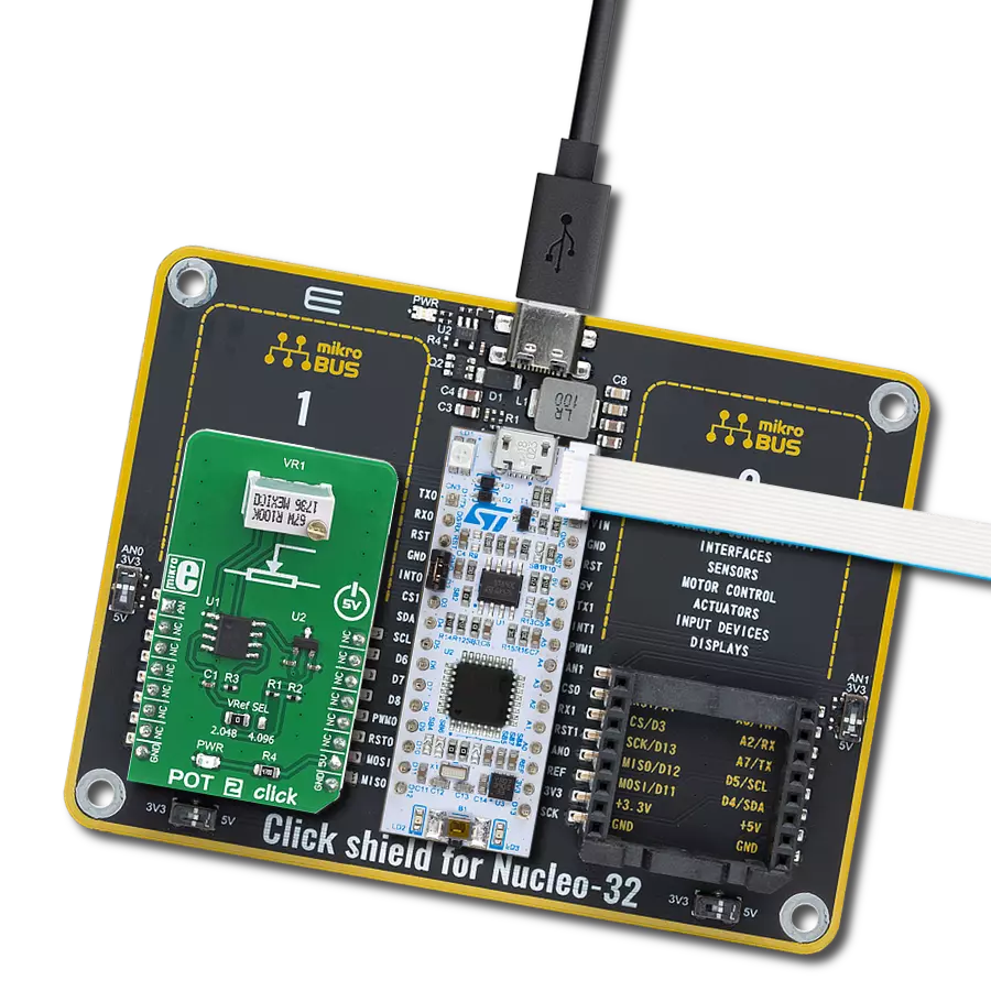
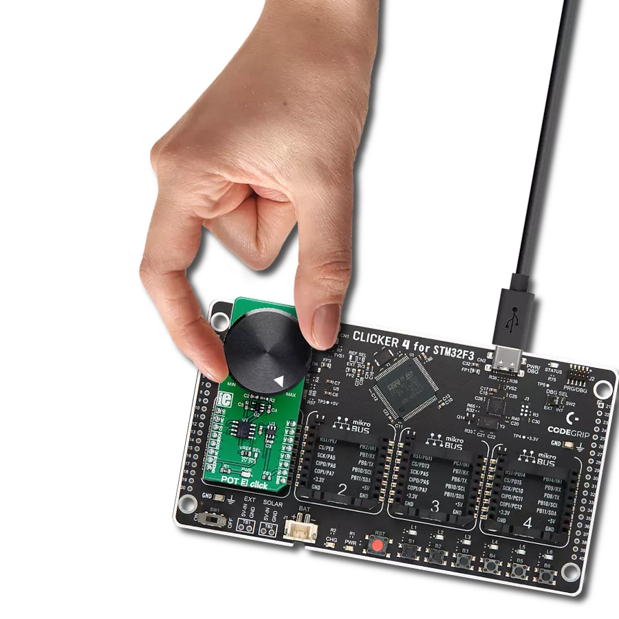
POT 2 Click
Dev. board
Clicker 2 for Kinetis
Compiler
NECTO Studio
MCU
MK64FN1M0VDC12
Our trimmer potentiometers are meticulously crafted to deliver unparalleled precision, enabling you to calibrate and fine-tune your equipment with exceptional accuracy, so you can achieve peak performance effortlessly
A
A
Hardware Overview
How does it work?
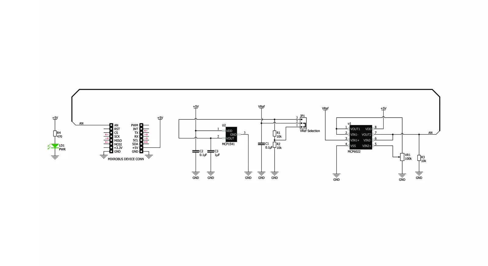
POT 2 Click is based on the MCP1541, a precision voltage reference IC from Microchip is used to provide the voltage of 4.096V. is fed to an input of an operational amplifier, that acts as the buffer, with the unity gain. The output of the first buffer is fed to one end of a high-precision trimmer-potentiometer. The second end of the potentiometer is grounded, while the middle tap of the potentiometer is used as the input to a second buffer. The output of the second buffer is routed to the AN pin of the mikroBUS™, allowing the host microcontroller (MCU) to use the output voltage for any purpose. The design uses the MCP6022, a dual, rail-to-rail operational amplifier from Microchip. This operational amplifier is a perfect choice for this design, as it allows rail-to-rail
operation, uses a single power supply of 5V, and has a stable unity gain. Without the buffers, the variable impedance would affect the reference voltage. The reference voltage IC can provide less than 10 mA, with the significant voltage drop for output currents exceeding 2 mA. Therefore, the MCP6022 used as a dual buffer ensures good stability of the circuit. The potentiometer itself is a multi-turn type of potentiometer which provides high accuracy. It is equipped with a screw, which can be rotated 20 times between the end positions. This allows the resistance to be precisely selected. The fact that the screw fits tightly into the casing of the potentiometer, ensures that no resistance variations are possible, unlike the conventional knob or slider potentiometers.
POT 2 click is equipped with the SMD jumper, which is used to select the voltage reference for the potentiometer. There are two options available: 2.048V and 4.096V. These values are the most commonly used voltage references for different kinds of A/D converters. Most MCUs which use 3.3V for the power supply, do not have the option to use 4.096V (full voltage output of the MCP1541 IC), so an option to select 2.048V by dividing the output voltage of the MCP1541 IC, is very useful in that case. The voltage reference can be selected by moving the SMD jumper labeled as VRef SEL to the desired position (2.048V or 4.096V).


Features overview
Development board
Clicker 2 for Kinetis is a compact starter development board that brings the flexibility of add-on Click boards™ to your favorite microcontroller, making it a perfect starter kit for implementing your ideas. It comes with an onboard 32-bit ARM Cortex-M4F microcontroller, the MK64FN1M0VDC12 from NXP Semiconductors, two mikroBUS™ sockets for Click board™ connectivity, a USB connector, LED indicators, buttons, a JTAG programmer connector, and two 26-pin headers for interfacing with external electronics. Its compact design with clear and easily recognizable silkscreen markings allows you to build gadgets with unique functionalities and
features quickly. Each part of the Clicker 2 for Kinetis development kit contains the components necessary for the most efficient operation of the same board. In addition to the possibility of choosing the Clicker 2 for Kinetis programming method, using a USB HID mikroBootloader or an external mikroProg connector for Kinetis programmer, the Clicker 2 board also includes a clean and regulated power supply module for the development kit. It provides two ways of board-powering; through the USB Micro-B cable, where onboard voltage regulators provide the appropriate voltage levels to each component on the board, or
using a Li-Polymer battery via an onboard battery connector. All communication methods that mikroBUS™ itself supports are on this board, including the well-established mikroBUS™ socket, reset button, and several user-configurable buttons and LED indicators. Clicker 2 for Kinetis is an integral part of the Mikroe ecosystem, allowing you to create a new application in minutes. Natively supported by Mikroe software tools, it covers many aspects of prototyping thanks to a considerable number of different Click boards™ (over a thousand boards), the number of which is growing every day.

Microcontroller Overview
MCU Card / MCU

Architecture
ARM Cortex-M4
MCU Memory (KB)
1024
Silicon Vendor
NXP
Pin count
121
RAM (Bytes)
262144
Used MCU Pins
mikroBUS™ mapper
Take a closer look
Click board™ Schematic
Step by step
Project assembly

Start by selecting your development board and Click board™. Begin with the Clicker 2 for Kinetis as your development board.


Software Support
Library Description
This library contains API for POT 2 Click driver.
Key functions:
pot2_generic_read- Generic read function
Open Source
Code example
The complete application code and a ready-to-use project are available through the NECTO Studio Package Manager for direct installation in the NECTO Studio. The application code can also be found on the MIKROE GitHub account.
/*!
 * \file
 * \brief Pot2 Click example
 *
 * # Description
 * This demo-app shows the ADC values using POT 2 Click board.
 *
 * The demo application is composed of two sections :
 *
 * ## Application Init
 * Configures Clicks and log objects.
 *
 * ## Application Task
 * Demo app reads ADC data and displays them as dec and hex values every second
 *
 * \author Jovan Stajkovic
 *
 */
// ------------------------------------------------------------------- INCLUDES

#include "board.h"
#include "log.h"
#include "pot2.h"

// ------------------------------------------------------------------ VARIABLES

static pot2_t pot2;
static log_t logger;

static uint16_t adc_val;
static float voltage_val;

// ------------------------------------------------------ APPLICATION FUNCTIONS

void application_init ( void )
{
    log_cfg_t log_cfg;
    pot2_cfg_t cfg;

    /**
     * Logger initialization.
     * Default baud rate: 115200
     * Default log level: LOG_LEVEL_DEBUG
     * @note If USB_UART_RX and USB_UART_TX
     * are defined as HAL_PIN_NC, you will
     * need to define them manually for log to work.
     * See @b LOG_MAP_USB_UART macro definition for detailed explanation.
     */
    LOG_MAP_USB_UART( log_cfg );
    log_init( &logger, &log_cfg );
    log_info( &logger, "---- Application Init ----" );

    //  Click initialization.

    pot2_cfg_setup( &cfg );
    POT2_MAP_MIKROBUS( cfg, MIKROBUS_1 );
    if ( pot2_init( &pot2, &cfg ) == ADC_ERROR )
    {
        log_info( &logger, "---- Application Init Error ----" );
        log_info( &logger, "---- Please, run program again ----" );

        for ( ; ; );
    }
    log_info( &logger, "---- Application Init Done ----\r\n" );

    voltage_val = 0;
    adc_val = 0;
}

void application_task ( void )
{
    if ( pot2_read_adc ( &pot2, &adc_val ) != ADC_ERROR )
    {
        log_printf( &logger, " ADC value : [DEC] %u, [HEX] 0x%x\r\n", adc_val, adc_val );
    }

    if ( pot2_read_pin_voltage ( &pot2, &voltage_val ) != ADC_ERROR )
    {
        log_printf( &logger, " Voltage value : %.2f\r\n", voltage_val );
    }

    log_printf( &logger, "------------------------------------------\r\n" );
    Delay_ms ( 1000 );
}

int main ( void )
{
    /* Do not remove this line or clock might not be set correctly. */
    #ifdef PREINIT_SUPPORTED
    preinit();
    #endif

    application_init( );

    for ( ; ; )
    {
        application_task( );
    }

    return 0;
}


// ------------------------------------------------------------------------ END