Generate high-frequency clock output with ICS501 and PIC18F47Q10
Phase-Locked Loop (PLL) mechanism
Published Aug 09, 2023
Click board™
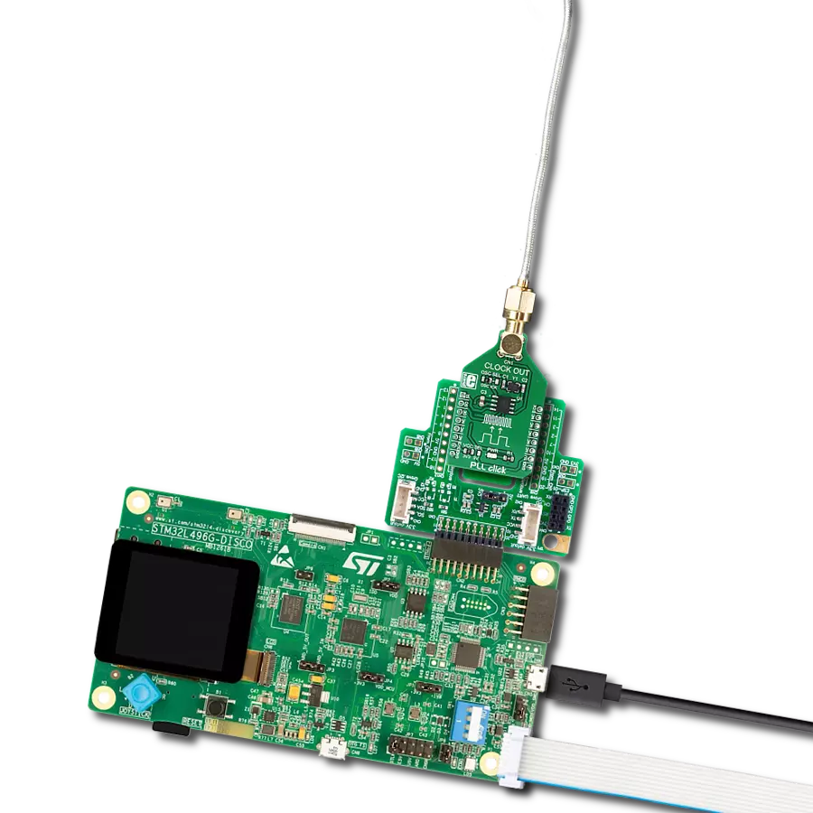
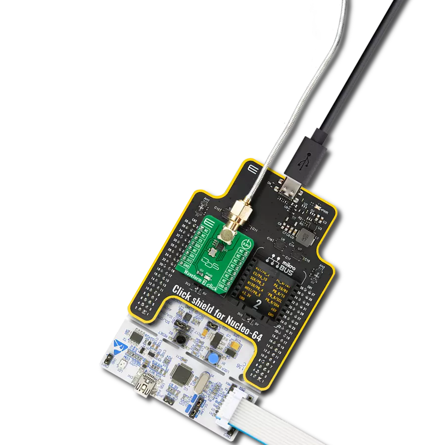
PLL Click
Dev. board
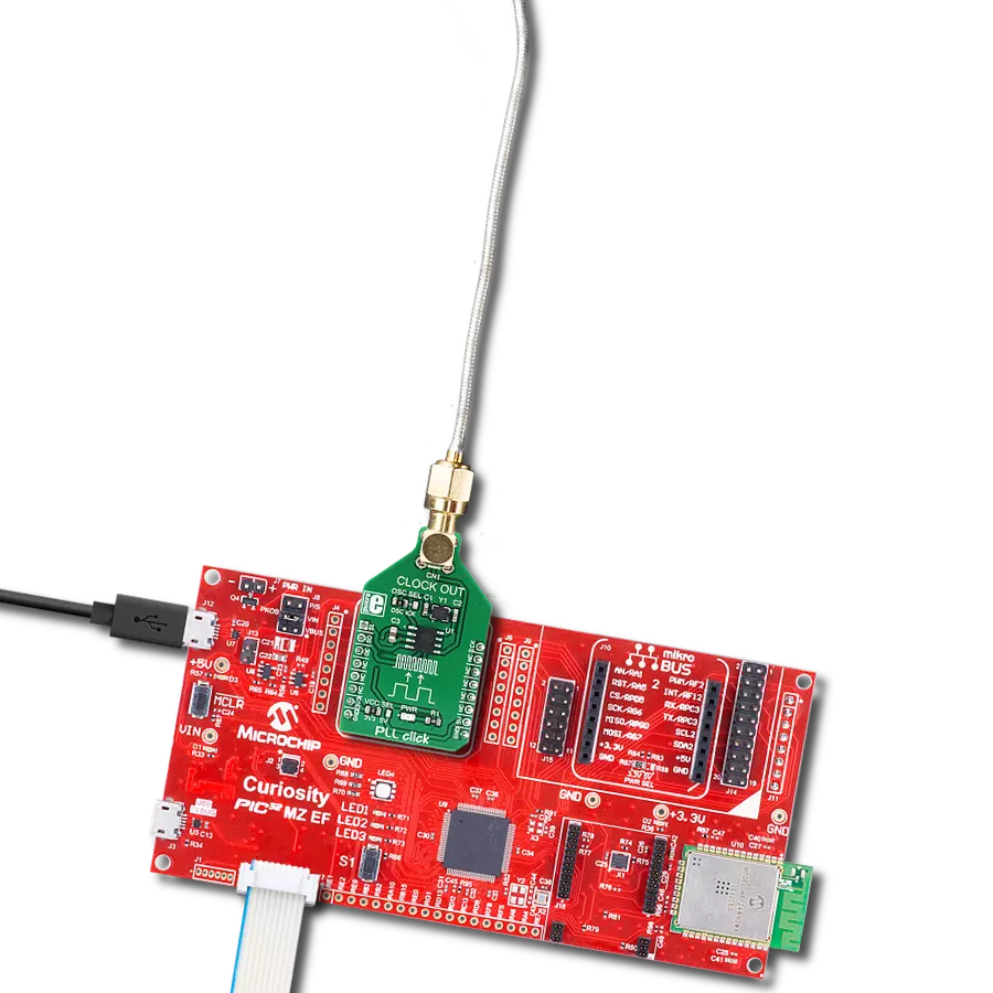
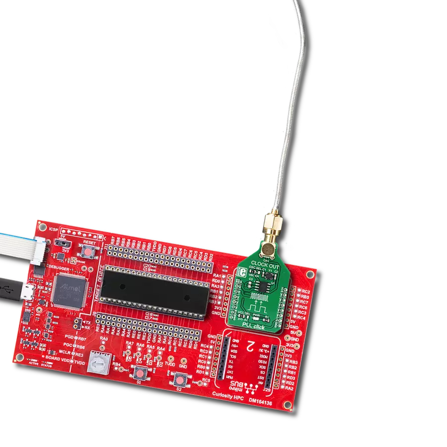
Curiosity HPC
Compiler
NECTO Studio
MCU
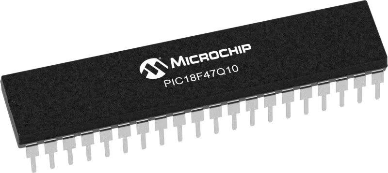
PIC18F47Q10
Generate highly stable and coherent high-frequency signals for applications requiring tight synchronization and minimal phase noise
A
A
Hardware Overview
How does it work?
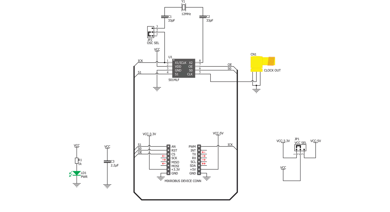
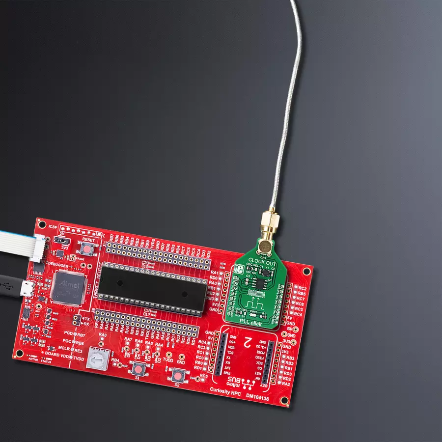
PLL Click is based on the ICS501, a LOCO™ PLL clock multiplier, from Integrated Device Technology. This IC uses the Phase-Locked Loop to provide a high-frequency clock output, deriving input from a much cheaper, standard fundamental frequency crystal oscillator. Besides the onboard crystal oscillator fixed at 12MHz, it is possible to select the signal from the mikroBUS™ PWM pin as the clock input source. To select the desired multiplication factor, the states of the two input pins, S0 and S1, are routed to the mikroBUS™ pins RST and AN, respectively. These pins can be set to a HIGH or LOW logic state or disconnected (by tri-stating the MCU pins). The combination of these pins states will set the PLL
Click to a specific multiplier. The Output Enable (OE) pin of the ICS501 is used to turn off the output clock by setting it to a LOW logic level. It will additionally set the clock output pin in high impedance (Hi-Z) mode, allowing complete disconnection and no influence on the rest of the circuit, which is useful for experimenting and prototyping purposes. This pin is internally pulled to a HIGH logic level. The OE pin is routed to the CS pin of the mikroBUS™. PLL Click is equipped with two onboard SMD jumpers. The SMD jumper labeled as the VCC SEL is used to select the operating voltage level, consequently limiting the amplitude of the clock output signal with respect to the selected voltage. The other SMD jumper
labeled as the OSC SEL chooses the clock input source between the onboard 12MHz crystal oscillator or the external clock signal. The output signal is routed through the onboard SMA connector, which provides a secure connection and good signal shielding. PLL Click has a library containing functions for all the MIKROE compilers (mikroBASIC, mikroPASCAL, and mikroC). Although relatively easy to control, the library offers comprehensive functions that make the code readable and easy to use. The included example application demonstrates the use of these functions, and it can be used as a reference for custom projects.

Features overview
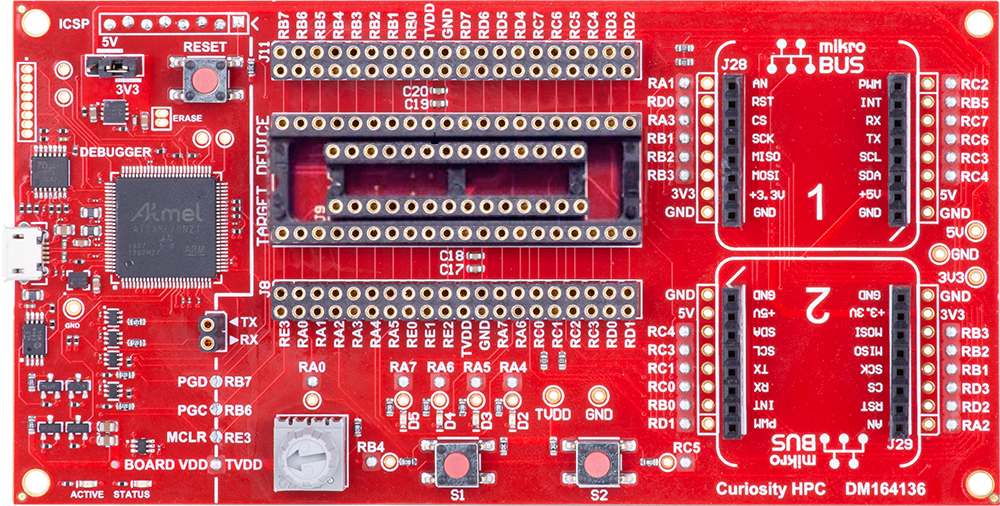
Development board
Curiosity HPC, standing for Curiosity High Pin Count (HPC) development board, supports 28- and 40-pin 8-bit PIC MCUs specially designed by Microchip for the needs of rapid development of embedded applications. This board has two unique PDIP sockets, surrounded by dual-row expansion headers, allowing connectivity to all pins on the populated PIC MCUs. It also contains a powerful onboard PICkit™ (PKOB), eliminating the need for an external programming/debugging tool, two mikroBUS™ sockets for Click board™ connectivity, a USB connector, a set of indicator LEDs, push button switches and a variable potentiometer. All
these features allow you to combine the strength of Microchip and Mikroe and create custom electronic solutions more efficiently than ever. Each part of the Curiosity HPC development board contains the components necessary for the most efficient operation of the same board. An integrated onboard PICkit™ (PKOB) allows low-voltage programming and in-circuit debugging for all supported devices. When used with the MPLAB® X Integrated Development Environment (IDE, version 3.0 or higher) or MPLAB® Xpress IDE, in-circuit debugging allows users to run, modify, and troubleshoot their custom software and hardware
quickly without the need for additional debugging tools. Besides, it includes a clean and regulated power supply block for the development board via the USB Micro-B connector, alongside all communication methods that mikroBUS™ itself supports. Curiosity HPC development board allows you to create a new application in just a few steps. Natively supported by Microchip software tools, it covers many aspects of prototyping thanks to many number of different Click boards™ (over a thousand boards), the number of which is growing daily.

Microcontroller Overview
MCU Card / MCU
Architecture
PIC
MCU Memory (KB)
128
Silicon Vendor
Microchip
Pin count
40
RAM (Bytes)
3615
Used MCU Pins
mikroBUS™ mapper
Take a closer look
Click board™ Schematic
Step by step
Project assembly
Start by selecting your development board and Click board™. Begin with the Curiosity HPC as your development board.


Software Support
Library Description
This library contains API for PLL Click driver.
Key functions:
pll_set_clock_output- This function settings clock outputpll_set_pll_4x- This function settings PLL x4pll_set_pll_6x- This function settings PLL x6
Open Source
Code example
The complete application code and a ready-to-use project are available through the NECTO Studio Package Manager for direct installation in the NECTO Studio. The application code can also be found on the MIKROE GitHub account.
/*!
 * \file
 * \brief PLL Click example
 *
 * # Description
 * This app sets PLL signals.
 *
 * The demo application is composed of two sections :
 *
 * ## Application Init
 * Initializes device.
 *
 * ## Application Task
 * Every 2 seconds, the PLL increases the input clock from min (x2) to max (x8) level.
 *
 * \author MikroE Team
 *
 */
// ------------------------------------------------------------------- INCLUDES

#include "board.h"
#include "log.h"
#include "pll.h"

// ------------------------------------------------------------------ VARIABLES

static pll_t pll;
static log_t logger;

// ------------------------------------------------------ APPLICATION FUNCTIONS

void application_init ( void )
{
    log_cfg_t log_cfg;
    pll_cfg_t cfg;

    /**
     * Logger initialization.
     * Default baud rate: 115200
     * Default log level: LOG_LEVEL_DEBUG
     * @note If USB_UART_RX and USB_UART_TX
     * are defined as HAL_PIN_NC, you will
     * need to define them manually for log to work.
     * See @b LOG_MAP_USB_UART macro definition for detailed explanation.
     */
    LOG_MAP_USB_UART( log_cfg );
    log_init( &logger, &log_cfg );
    log_info( &logger, "---- Application Init ----" );

    //  Click initialization.
    pll_cfg_setup( &cfg );
    PLL_MAP_MIKROBUS( cfg, MIKROBUS_1 );
    pll_init( &pll, &cfg );
    pll_set_clock_output( &pll, PLL_CLOCK_ENABLE );
}

void application_task ( void )
{
    log_printf( &logger, " PLL level: x2\r\n\n" );
    pll_set_pll_2x( &pll );
    Delay_ms ( 1000 );
    Delay_ms ( 1000 );
    log_printf( &logger, " PLL level: x3\r\n\n" );
    pll_set_pll_3x( &pll );
    Delay_ms ( 1000 );
    Delay_ms ( 1000 );
    log_printf( &logger, " PLL level: x3.125\r\n\n" );
    pll_set_pll_3_125x( &pll );
    Delay_ms ( 1000 );
    Delay_ms ( 1000 );
    log_printf( &logger, " PLL level: x4\r\n\n" );
    pll_set_pll_4x( &pll );
    Delay_ms ( 1000 );
    Delay_ms ( 1000 );
    log_printf( &logger, " PLL level: x5\r\n\n" );
    pll_set_pll_5x( &pll );
    Delay_ms ( 1000 );
    Delay_ms ( 1000 );
    log_printf( &logger, " PLL level: x5.3125\r\n\n" );
    pll_set_pll_5_3125x( &pll );
    Delay_ms ( 1000 );
    Delay_ms ( 1000 );
    log_printf( &logger, " PLL level: x6\r\n\n" );
    pll_set_pll_6x( &pll );
    Delay_ms ( 1000 );
    Delay_ms ( 1000 );
    log_printf( &logger, " PLL level: x6.25\r\n\n" );
    pll_set_pll_6_25x( &pll );
    Delay_ms ( 1000 );
    Delay_ms ( 1000 );
    log_printf( &logger, " PLL level: x8\r\n\n" );
    pll_set_pll_8x( &pll );
    Delay_ms ( 1000 );
    Delay_ms ( 1000 );
}

int main ( void )
{
    /* Do not remove this line or clock might not be set correctly. */
    #ifdef PREINIT_SUPPORTED
    preinit();
    #endif

    application_init( );

    for ( ; ; )
    {
        application_task( );
    }

    return 0;
}

// ------------------------------------------------------------------------ END
Additional Support
Resources
Category:Clock generator