Say goodbye to data loss worries with CY14B101I and PIC32MZ2048EFH100
nvSRAM: Where data lives forever

Published Oct 28, 2023
Click board™
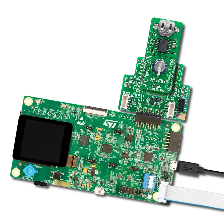
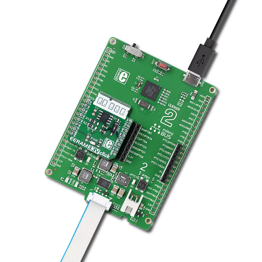
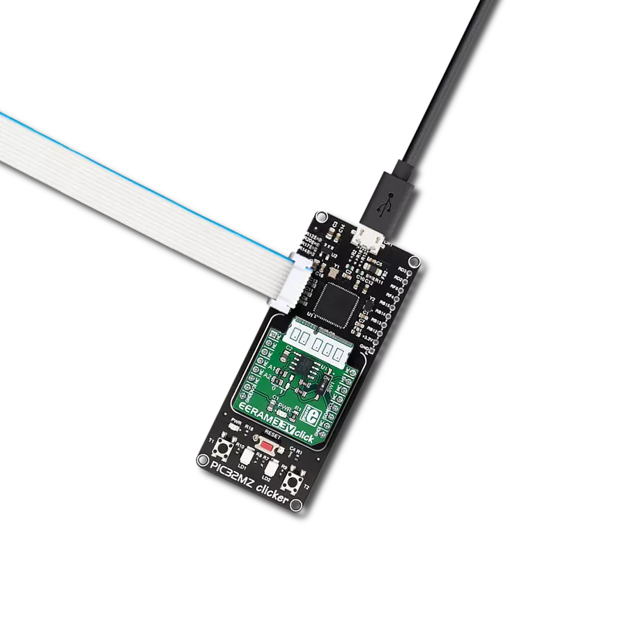
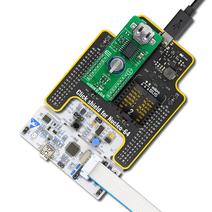
nvSRAM 3 Click
Dev. board
Flip&Click PIC32MZ
Compiler
NECTO Studio
MCU
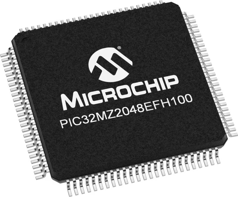
PIC32MZ2048EFH100
Trust nvSRAM as your data's timeless vault, ensuring that precious memories stay alive and intact
A
A
Hardware Overview
How does it work?
nvSRAM 3 Click as its foundation uses the CY14B101I, a 1-Mbit nvSRAM organized as 128K words of 8 bits each with a fully-featured real-time clock from Infineon. The CY14B101I specifies one million endurance cycles for cells with data retention of a minimum of 20 years, while the QuantumTrap cells provide highly reliable, nonvolatile data storage. In system power loss, data from the SRAM is automatically transferred to its nonvolatile cell using energy stored in a capacitor labeled as C2. During the Power-Up, data from the nonvolatile cell is recalled automatically in the SRAM array and available to the user. The endurance cycle consumes when data transfer happens from the SRAM cells to nonvolatile cells during the Power-Down. This Click board™ can be permanently powered by placing jumpers labeled as RTC-CAP or RTC-BATT. The CY14B101I uses an external battery power source from the button cell battery holder by utilizing an automatic backup. It is suitable for
12mm Coin Cell batteries when there is no power supply on its main power terminals, allowing for uninterrupted operation. nvSRAM 3 Click communicates with MCU using a standard I2C 2-Wire interface, with clock frequencies up to 100kHz in the Standard, 400kHz in the Fast, 1MHz in FastPlus, and up to 3.4MHz in High-Speed Mode. The CY14B101I offers zero cycle delay write operation with infinite SRAM write endurance. It also allows the choice of the least significant bit (LSB) of its I2C slave address by positioning SMD jumpers labeled ADDR SEL to an appropriate position marked as 0 and 1. An additional feature of this Click board™ represents the Write Protection and Interrupt functions labeled as WP and INT routed on the PWM and INT pins of the mikroBUS™ socket. The WP pin is an active-high pin that protects the entire memory and all registers from write operations. MCU must hold the WP pin high to inhibit all the write operations. When this pin is high, all memory and register
writes are prohibited, and the address counter does not increment. On the other hand, the CY14B101I can use an INT pin in several ways, such as interrupt output, calibration, or a square wave, programmable to respond to the clock alarm, the watchdog timer, and the power monitor. The STORE operation of the CY14B101I can be controlled and acknowledged via the HSB pin, routed on the RST pin of the mikroBUS™ socket. If no STORE/RECALL is in progress, the CY14B101I can use this pin to request a hardware STORE cycle. When the HSB pin is in a LOW logic state, the CY14B101I conditionally initiates a STORE operation. This Click board™ can be operated only with a 3.3V logic voltage level. The board must perform appropriate logic voltage level conversion before using MCUs with different logic levels. Also, it comes equipped with a library containing functions and an example code that can be used for further development.

Features overview
Development board
Flip&Click PIC32MZ is a compact development board designed as a complete solution that brings the flexibility of add-on Click boards™ to your favorite microcontroller, making it a perfect starter kit for implementing your ideas. It comes with an onboard 32-bit PIC32MZ microcontroller, the PIC32MZ2048EFH100 from Microchip, four mikroBUS™ sockets for Click board™ connectivity, two USB connectors, LED indicators, buttons, debugger/programmer connectors, and two headers compatible with Arduino-UNO pinout. Thanks to innovative manufacturing technology,
it allows you to build gadgets with unique functionalities and features quickly. Each part of the Flip&Click PIC32MZ development kit contains the components necessary for the most efficient operation of the same board. In addition, there is the possibility of choosing the Flip&Click PIC32MZ programming method, using the chipKIT bootloader (Arduino-style development environment) or our USB HID bootloader using mikroC, mikroBasic, and mikroPascal for PIC32. This kit includes a clean and regulated power supply block through the USB Type-C (USB-C) connector. All communication
methods that mikroBUS™ itself supports are on this board, including the well-established mikroBUS™ socket, user-configurable buttons, and LED indicators. Flip&Click PIC32MZ development kit allows you to create a new application in minutes. Natively supported by Mikroe software tools, it covers many aspects of prototyping thanks to a considerable number of different Click boards™ (over a thousand boards), the number of which is growing every day.

Microcontroller Overview
MCU Card / MCU
Architecture
PIC32
MCU Memory (KB)
2048
Silicon Vendor
Microchip
Pin count
100
RAM (Bytes)
524288
Used MCU Pins
mikroBUS™ mapper
Take a closer look
Click board™ Schematic

Step by step
Project assembly

Start by selecting your development board and Click board™. Begin with the Flip&Click PIC32MZ as your development board.


Software Support
Library Description
This library contains API for nvSRAM 3 Click driver.
Key functions:
nvsram3_memory_write- This function write a desired number of data bytes starting from the selected memory address by using I2C serial interface.nvsram3_memory_read- This function reads a desired number of data bytes starting from the selected memory address by using I2C serial interface.nvsram3_get_rtc_time- This function get RTC time data structure.
Open Source
Code example
The complete application code and a ready-to-use project are available through the NECTO Studio Package Manager for direct installation in the NECTO Studio. The application code can also be found on the MIKROE GitHub account.
/*!
 * @file main.c
 * @brief nvSRAM3 Click example
 *
 * # Description
 * The demo application shows how to write/read data to/from nvSRAM memory.
 * It also sets RTC date and time, then reads it in an infinite loop and displays results on USB UART each second.
 *
 * The demo application is composed of two sections :
 *
 * ## Application Init
 * Initializes device, reads the device ID, writes desired message to memory and sets RTC date and time.
 *
 * ## Application Task
 * Reads current date and time and then reads the message that we have previusly stored in the memory.
 * All data is being logged on USB UART.
 *
 * @author Stefan Filipovic
 *
 */

#include "board.h"
#include "log.h"
#include "nvsram3.h"

static nvsram3_t nvsram3;
static log_t logger;

static char demo_data[ 9 ] = { 'M', 'i', 'k', 'r', 'o', 'E', 13 ,10 , 0 };
static char rx_data[ 9 ];
static uint32_t memory_addr;
static uint8_t new_sec = 255;
static uint16_t c_year = 2020;

static nvsram3_rtc_time_t time;
static nvsram3_rtc_date_t date;

void application_init ( void )
{
    log_cfg_t log_cfg;  /**< Logger config object. */
    nvsram3_cfg_t nvsram3_cfg;  /**< Click config object. */

    /**
     * Logger initialization.
     * Default baud rate: 115200
     * Default log level: LOG_LEVEL_DEBUG
     * @note If USB_UART_RX and USB_UART_TX
     * are defined as HAL_PIN_NC, you will
     * need to define them manually for log to work.
     * See @b LOG_MAP_USB_UART macro definition for detailed explanation.
     */
    LOG_MAP_USB_UART( log_cfg );
    log_init( &logger, &log_cfg );
    log_info( &logger, " Application Init " );

    // Click initialization.

    nvsram3_cfg_setup( &nvsram3_cfg );
    NVSRAM3_MAP_MIKROBUS( nvsram3_cfg, MIKROBUS_1 );
    err_t init_flag = nvsram3_init( &nvsram3, &nvsram3_cfg );

    if ( init_flag == I2C_MASTER_ERROR )
    {
        log_error( &logger, " Application Init Error. " );
        log_info( &logger, " Please, run program again... " );

        for ( ; ; );
    }

    log_printf( &logger, "-----------------------\r\n" );
    log_printf( &logger, "     nvSRAM 3 Click    \r\n" );
    log_printf( &logger, "-----------------------\r\n" );

    nvsram3_default_cfg ( &nvsram3 );
    Delay_ms ( 100 );

    log_printf( &logger, " DEVICE ID: 0x%.8LX\r\n", nvsram3_get_device_id( &nvsram3 ) );
    log_printf( &logger, "-----------------------\r\n" );
    Delay_ms ( 100 );

    memory_addr = 0x10000;

    log_printf( &logger, "  Write data : %s", demo_data );
    nvsram3_memory_write( &nvsram3, memory_addr, &demo_data[ 0 ], 9 );
    log_printf( &logger, "-----------------------\r\n" );
    Delay_ms ( 1000 );

    date.day_of_week = 4;
    date.day = 31;
    date.month = 12;
    date.year = 2020;
    nvsram3_set_rtc_date( &nvsram3, date );
    Delay_ms ( 100 );

    time.hours = 23;
    time.min = 59;
    time.sec = 50;
    nvsram3_set_rtc_time( &nvsram3, time );
    Delay_ms ( 100 );
}

void application_task ( void )
{
    nvsram3_get_rtc_time( &nvsram3, &time );
    nvsram3_get_rtc_date( &nvsram3, &date );

    if ( time.sec != new_sec )
    {
        log_printf( &logger, "  Date      : %.2d-%.2d-%.4d\r\n", ( uint16_t ) date.day, ( uint16_t ) date.month, ( uint16_t ) date.year );
        log_printf( &logger, "  Time      : %.2d:%.2d:%.2d\r\n", ( uint16_t ) time.hours, ( uint16_t ) time.min, ( uint16_t ) time.sec );
        log_printf( &logger, "- - - - - - - - - - - - - - -\r\n" );
        new_sec = time.sec;

        if ( date.year != c_year )
        {
            log_printf( &logger, "     Happy New Year    \r\n" );
            c_year = date.year;
        }
        else
        {
            nvsram3_memory_read( &nvsram3, memory_addr, &rx_data[ 0 ], 9 );
            log_printf( &logger, "  Read data : %s", rx_data );
        }

        log_printf( &logger, "-----------------------\r\n" );
    }
    else
    {
        Delay_ms ( 500 );
    }
}

int main ( void )
{
    /* Do not remove this line or clock might not be set correctly. */
    #ifdef PREINIT_SUPPORTED
    preinit();
    #endif

    application_init( );

    for ( ; ; )
    {
        application_task( );
    }

    return 0;
}

// ------------------------------------------------------------------------ END
Additional Support
Resources
Category:SRAM