Ensure a stable and reliable output voltage with minimal dropout with TPS7A83A and PIC32MZ2048EFM100
Unlocking efficiency in voltage control

Published Sep 13, 2023
Click board™
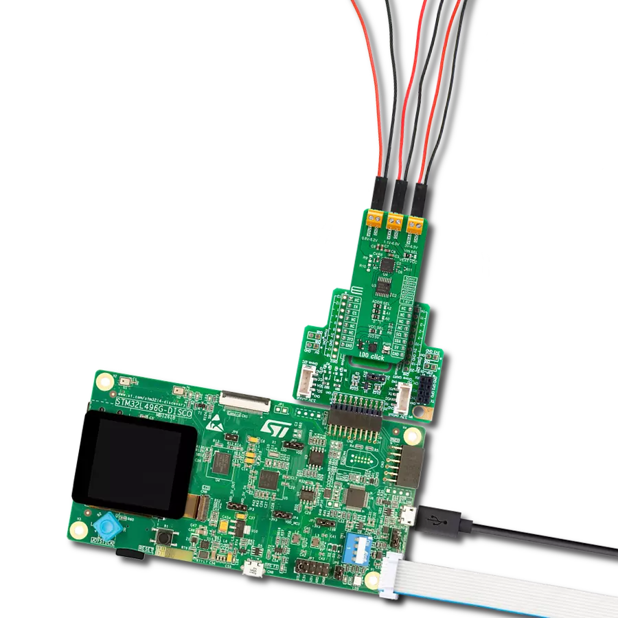
LDO Click
Dev. board
Curiosity PIC32 MZ EF
Compiler
NECTO Studio
MCU
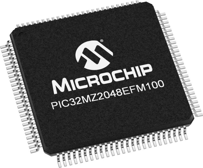
PIC32MZ2048EFM100
Witness voltage precision and dropout perfection with LDO regulators that set the standard for accurate and efficient voltage control
A
A
Hardware Overview
How does it work?
LDO Click is based on the TPS7A83A, a high-current (2A), low-noise, high-accuracy, and low-dropout linear voltage regulator from Texas Instruments. The TPS7A83A has several features that make it useful in various applications, like high accuracy, high-PSR output, and fast transient response for voltage regulation part, as well as certain internal protections like thermal shutdown and foldback current limit. All these features make this Click board™ a robust solution for many challenging problems in generating a clean, accurate power supply. The TPS7A8300A can be easily enabled using the EN pin of the mikroBUS™ socket, offering a switch operation to turn ON/OFF the TPS7A8300A. It has a pin-programmable output voltage from 0.8V-3.95V with a 50mV resolution, or it can be adjustable from 0.8V-5.2V using an external resistor divider (R9 and R10). The
pin-programmable output voltage is possible thanks to the TCA9534A, an I2C-configurable I/O expander also from Texas Instruments, which, by setting the appropriate voltage setting pins on the TPS7A83A, which are connected to an internal feedback network, programs the regulated output voltage. The TCA9534A expander can also choose the least significant bit (LSB) of its I2C slave address by positioning SMD jumpers labeled ADDR SEL to an appropriate position marked as 0 and 1. The adjustable output voltage is achieved through voltage divider resistors whose corresponding values can be found in the datasheet table. One of the power terminals on the board is the VBIAS terminal, which minimizes the internal charge-pump noise when the internal voltage is clamped, thereby reducing the overall output noise floor. This rail enables the use of
low-input voltage, low-output (LILO) voltage conditions (VEXT=1.2V, VOUT =1V) to reduce the power dissipation of the TPS7A8300A. Using a VBIAS voltage improves DC and AC performance for VEXT≤2.2V. This Click board™ can operate with either 3.3V or 5V logic voltage levels selected via the VCC SEL jumper. This way, it is allowed for both 3.3V and 5V capable MCUs to use the communication lines properly. Additionally, there is a possibility for the TPS7A83A power supply selection via jumper labeled as VIN SEL to supply the TPS7A83A from an external power supply terminal in the range from 1.1V to 6.5V or with selected mikroBUS™ power rail. However, the Click board™ comes equipped with a library containing easy-to-use functions and an example code that can be used as a reference for further development.

Features overview
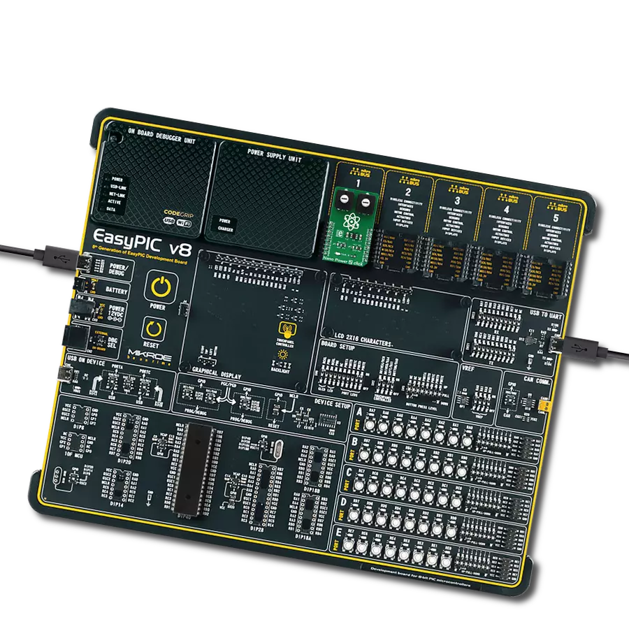
Development board
Curiosity PIC32 MZ EF development board is a fully integrated 32-bit development platform featuring the high-performance PIC32MZ EF Series (PIC32MZ2048EFM) that has a 2MB Flash, 512KB RAM, integrated FPU, Crypto accelerator, and excellent connectivity options. It includes an integrated programmer and debugger, requiring no additional hardware. Users can expand
functionality through MIKROE mikroBUS™ Click™ adapter boards, add Ethernet connectivity with the Microchip PHY daughter board, add WiFi connectivity capability using the Microchip expansions boards, and add audio input and output capability with Microchip audio daughter boards. These boards are fully integrated into PIC32’s powerful software framework, MPLAB Harmony,
which provides a flexible and modular interface to application development a rich set of inter-operable software stacks (TCP-IP, USB), and easy-to-use features. The Curiosity PIC32 MZ EF development board offers expansion capabilities making it an excellent choice for a rapid prototyping board in Connectivity, IOT, and general-purpose applications.

Microcontroller Overview
MCU Card / MCU
Architecture
PIC32
MCU Memory (KB)
2048
Silicon Vendor
Microchip
Pin count
100
RAM (Bytes)
524288
Used MCU Pins
mikroBUS™ mapper
Take a closer look
Click board™ Schematic

Step by step
Project assembly

Start by selecting your development board and Click board™. Begin with the Curiosity PIC32 MZ EF as your development board.


Track your results in real time
Application Output
1. Application Output - In Debug mode, the 'Application Output' window enables real-time data monitoring, offering direct insight into execution results. Ensure proper data display by configuring the environment correctly using the provided tutorial.

2. UART Terminal - Use the UART Terminal to monitor data transmission via a USB to UART converter, allowing direct communication between the Click board™ and your development system. Configure the baud rate and other serial settings according to your project's requirements to ensure proper functionality. For step-by-step setup instructions, refer to the provided tutorial.

3. Plot Output - The Plot feature offers a powerful way to visualize real-time sensor data, enabling trend analysis, debugging, and comparison of multiple data points. To set it up correctly, follow the provided tutorial, which includes a step-by-step example of using the Plot feature to display Click board™ readings. To use the Plot feature in your code, use the function: plot(*insert_graph_name*, variable_name);. This is a general format, and it is up to the user to replace 'insert_graph_name' with the actual graph name and 'variable_name' with the parameter to be displayed.

Software Support
Library Description
This library contains API for LDO Click driver.
Key functions:
ldo_enable_device- This function enables the device by setting the EN pin to HIGH logic stateldo_disable_device- This function disables the device by setting the EN pin to LOW logic stateldo_set_vout- This function sets the voltage output.
Open Source
Code example
The complete application code and a ready-to-use project are available through the NECTO Studio Package Manager for direct installation in the NECTO Studio. The application code can also be found on the MIKROE GitHub account.
/*!
 * @file main.c
 * @brief LDO Click example
 *
 * # Description
 * This example demonstrates the use of LDO Click by changing the output voltage.
 *
 * The demo application is composed of two sections :
 *
 * ## Application Init
 * Initializes the driver and performs the device default configuration.
 *
 * ## Application Task
 * Changes the output voltage every 3 seconds and displays on the USB UART
 * the currently set voltage output value.
 *
 * @note
 * In order to have up to 3950mV at VOUT you will need to move the VIN SEL on-board jumper
 * to the VEXT position and provide at least 3950mV voltage input at the VEXT terminal.
 * Otherwise, the maximum level of VOUT will be limited to 3.3V system voltage.
 *
 * @author Stefan Filipovic
 *
 */

#include "board.h"
#include "log.h"
#include "ldo.h"

static ldo_t ldo;
static log_t logger;

void application_init ( void )
{
    log_cfg_t log_cfg;  /**< Logger config object. */
    ldo_cfg_t ldo_cfg;  /**< Click config object. */

    /**
     * Logger initialization.
     * Default baud rate: 115200
     * Default log level: LOG_LEVEL_DEBUG
     * @note If USB_UART_RX and USB_UART_TX
     * are defined as HAL_PIN_NC, you will
     * need to define them manually for log to work.
     * See @b LOG_MAP_USB_UART macro definition for detailed explanation.
     */
    LOG_MAP_USB_UART( log_cfg );
    log_init( &logger, &log_cfg );
    log_info( &logger, " Application Init " );

    // Click initialization.
    ldo_cfg_setup( &ldo_cfg );
    LDO_MAP_MIKROBUS( ldo_cfg, MIKROBUS_1 );
    if ( I2C_MASTER_ERROR == ldo_init( &ldo, &ldo_cfg ) )
    {
        log_error( &logger, " Communication init." );
        for ( ; ; );
    }

    if ( LDO_ERROR == ldo_default_cfg ( &ldo ) )
    {
        log_error( &logger, " Default configuration." );
        for ( ; ; );
    }

    log_info( &logger, " Application Task " );
}

void application_task ( void )
{
    static uint16_t vout = LDO_VOUT_MIN;
    if ( LDO_OK == ldo_set_vout ( &ldo, vout ) )
    {
        log_printf ( &logger, " VOUT: %u mV\r\n\n", vout );
    }
    vout += LDO_VOUT_STEP;
    if ( vout > LDO_VOUT_MAX )
    {
        vout = LDO_VOUT_MIN;
    }
    Delay_ms ( 1000 );
    Delay_ms ( 1000 );
    Delay_ms ( 1000 );
}

int main ( void )
{
    /* Do not remove this line or clock might not be set correctly. */
    #ifdef PREINIT_SUPPORTED
    preinit();
    #endif

    application_init( );

    for ( ; ; )
    {
        application_task( );
    }

    return 0;
}

// ------------------------------------------------------------------------ END