Safeguard sensitive information through reliable flash memory, the W25N01GVZEIG combined with PIC18F2515
Where speed meets storage brilliance
Published Nov 01, 2023
Click board™
Flash 5 Click
Dev. board
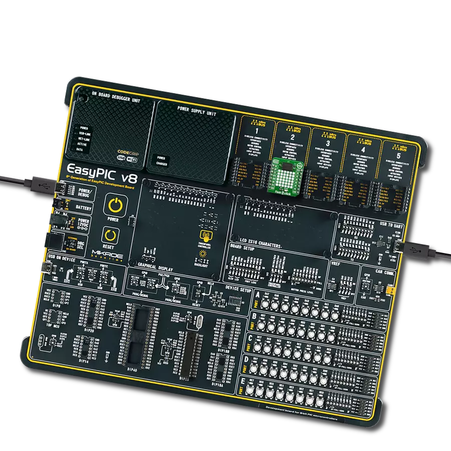
EasyPIC v8
Compiler
NECTO Studio
MCU
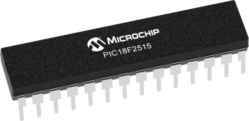
PIC18F2515
Ensure reliable data retention and encryption through our flash memory solution
A
A
Hardware Overview
How does it work?
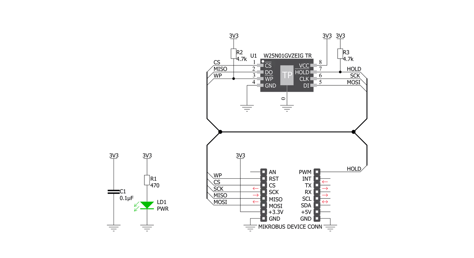
Flash 5 Click is based on the W25N01GVZEIG/IT (1G-bit) Serial SLC NAND Flash Memory from Winbond. The device operates on a single 3.3V power supply with current consumption as low as 25mA active and 10µA for standby. All W25N SpiFlash family devices are offered in space-saving packages, which were previously impossible to use for the typical NAND flash memory. The W25N01GVZEIG/IT 1G-bit memory array is organized into 65,536 programmable pages of 2,048 bytes each. The entire page can be programmed simultaneously using the data from the 2,048-Byte internal buffer. Pages can be erased in groups of 64 (128KB block erase). The W25N01GVZEIG/IT has 1,024 erasable blocks. The Flash 5 Click uses the standard Serial Peripheral Interface (SPI), supporting SPI clock frequencies of up to 104MHz. Besides that, the W25N01GVZEIG/IT provides a new Continuous Read Mode that allows for efficient access to the entire memory array with a single Read command. This feature is ideal
for code-shadowing applications. Also, it offers the highest performance thanks to the Serial NAND Flash with 104MHz Standard/Dual/Quad SPI clocks and a 50MB/S continuous data transfer rate. Given that it has an efficient “Continuous Read Mode,” it allows direct read access to the entire array. However, the performance depends on the main MCU used with this Click board™. A Hold pin, Write Protect pin and programmable write protection provide further control flexibility. Additionally, the device supports JEDEC standard manufacturer and device ID, one 2,048-Byte Unique ID page, one 2,048-Byte parameter page, and ten 2,048-Byte OTP pages. To provide better NAND flash memory manageability, user-configurable internal ECC and bad block management are also available in W25N01GVZEIG/IT. The W25N01GVZEIG/IT is accessed through an SPI-compatible bus consisting of four signals: Serial Clock (CLK), Chip Select (/CS), Serial Data Input (DI), and Serial Data
Output (DO). Standard SPI instructions use the DI input pin to serially write instructions, addresses, or data to the device on the rising edge of CLK. The DO output pin reads data or status from the device on the falling edge of CLK. For a detailed explanation, please consult the included datasheet. However, MikroElektronika provides a library that contains functions that simplify and speed up working with this device. The provided application example demonstrates the functionality of the library functions. It can be used as a reference for a custom project development. This Click board™ can be operated only with a 3.3V logic voltage level. The board must perform appropriate logic voltage level conversion before using MCUs with different logic levels. Also, it comes equipped with a library containing functions and an example code that can be used, as a reference, for further development.


Features overview
Development board
EasyPIC v8 is a development board specially designed for the needs of rapid development of embedded applications. It supports many high pin count 8-bit PIC microcontrollers from Microchip, regardless of their number of pins, and a broad set of unique functions, such as the first-ever embedded debugger/programmer. The development board is well organized and designed so that the end-user has all the necessary elements, such as switches, buttons, indicators, connectors, and others, in one place. Thanks to innovative manufacturing technology, EasyPIC v8 provides a fluid and immersive working experience, allowing access anywhere and under any
circumstances at any time. Each part of the EasyPIC v8 development board contains the components necessary for the most efficient operation of the same board. In addition to the advanced integrated CODEGRIP programmer/debugger module, which offers many valuable programming/debugging options and seamless integration with the Mikroe software environment, the board also includes a clean and regulated power supply module for the development board. It can use a wide range of external power sources, including a battery, an external 12V power supply, and a power source via the USB Type-C (USB-C) connector.
Communication options such as USB-UART, USB DEVICE, and CAN are also included, including the well-established mikroBUS™ standard, two display options (graphical and character-based LCD), and several different DIP sockets. These sockets cover a wide range of 8-bit PIC MCUs, from the smallest PIC MCU devices with only eight up to forty pins. EasyPIC v8 is an integral part of the Mikroe ecosystem for rapid development. Natively supported by Mikroe software tools, it covers many aspects of prototyping and development thanks to a considerable number of different Click boards™ (over a thousand boards), the number of which is growing every day.

Microcontroller Overview
MCU Card / MCU
Architecture
PIC
MCU Memory (KB)
48
Silicon Vendor
Microchip
Pin count
28
RAM (Bytes)
3968
Used MCU Pins
mikroBUS™ mapper
Take a closer look
Click board™ Schematic
Step by step
Project assembly

Start by selecting your development board and Click board™. Begin with the EasyPIC v8 as your development board.


Software Support
Library Description
This library contains API for Flash 5 Click driver.
Key functions:
flash5_page_read- Function for setting page readflash5_page_load_memory- Function for loading one pageflash5_write_status_data- Function for writing status data
Open Source
Code example
The complete application code and a ready-to-use project are available through the NECTO Studio Package Manager for direct installation in the NECTO Studio. The application code can also be found on the MIKROE GitHub account.
/*!
 * \file
 * \brief Flash5 Click example
 *
 * # Description
 * This application is for storing mass storage.
 *
 * The demo application is composed of two sections :
 *
 * ## Application Init
 * Initializes driver, resets device, erasing one page of memory, tests communication and configures device.
 *
 * ## Application Task
 * Writes "MikroE" to device memory and then reads it and sends it to log.
 *
 * \author MikroE Team
 *
 */
// ------------------------------------------------------------------- INCLUDES

#include "board.h"
#include "log.h"
#include "flash5.h"

// ------------------------------------------------------------------ VARIABLES

static flash5_t flash5;
static log_t logger;
static char write_buf[ 7 ] = { 'M', 'i', 'k', 'r', 'o', 'E', 0 };

// ------------------------------------------------------ APPLICATION FUNCTIONS

void application_init ( void )
{
    log_cfg_t log_cfg;
    flash5_cfg_t cfg;
    uint8_t device_check = 0;

    /**
     * Logger initialization.
     * Default baud rate: 115200
     * Default log level: LOG_LEVEL_DEBUG
     * @note If USB_UART_RX and USB_UART_TX
     * are defined as HAL_PIN_NC, you will
     * need to define them manually for log to work.
     * See @b LOG_MAP_USB_UART macro definition for detailed explanation.
     */
    LOG_MAP_USB_UART( log_cfg );
    log_init( &logger, &log_cfg );
    log_info( &logger, "---- Application Init ----" );

    //  Click initialization.

    flash5_cfg_setup( &cfg );
    FLASH5_MAP_MIKROBUS( cfg, MIKROBUS_1 );
    flash5_init( &flash5, &cfg );

    log_printf( &logger, " - Reseting device... \r\n" );

    flash5_software_reset( &flash5 );
    Delay_ms ( 1000 );

    log_printf( &logger, " - Erasing memory... \r\n" );

    flash5_send_cmd( &flash5, FLASH5_CMD_WRITE_ENABLE );
    flash5_erase_page_data( &flash5, 0x0001 );

    device_check = flash5_device_id_check( &flash5 );

    if ( device_check == FLASH5_DEVICE_OK )
    {
        log_printf( &logger, " - Device OK \r\n" );
    }
    else
    {
        log_printf( &logger, " - Device Error \r\n" );
        for( ; ; );
    }
    Delay_ms ( 100 );

    log_printf( &logger, " - Configuring device \r\n" );

    flash5_write_status_data( &flash5, FLASH5_CMD_WRITE_REG_STATUS1, FLASH5_REG_STATUS_1, FLASH5_RS1_WRITE_PROTECTION_DISABLE |
                                                                                          FLASH5_RS1_SRP1_ENABLE );
    flash5_write_status_data( &flash5, FLASH5_CMD_WRITE_REG_STATUS1, FLASH5_REG_STATUS_1, FLASH5_RS2_PAGE_READ_MODE );
    Delay_ms ( 1000 );

    log_printf( &logger, "***** App init ***** \r\n" );
    log_printf( &logger, "------------------- \r\n" );
    Delay_ms ( 500 );
}

void application_task ( )
{
    char read_buf[ 6 ];
    uint8_t n_counter;

    flash5_send_cmd( &flash5, FLASH5_CMD_WRITE_ENABLE );
    flash5_page_load_memory( &flash5, 0x000A, &write_buf[ 0 ], 6 );
    flash5_page_read_memory( &flash5, 0x000A, &read_buf[ 0 ], 6 );

    for( n_counter = 0; n_counter < 6; n_counter++ )
    {
        log_printf( &logger, " %c ", read_buf[ n_counter ] );
        Delay_ms ( 100 );
    }

    log_printf( &logger, " \r\n" );
    log_printf( &logger, "------------------- \r\n" );
    Delay_ms ( 1000 );
    Delay_ms ( 1000 );
    Delay_ms ( 1000 );
    Delay_ms ( 1000 );
    Delay_ms ( 1000 );
}

int main ( void )
{
    /* Do not remove this line or clock might not be set correctly. */
    #ifdef PREINIT_SUPPORTED
    preinit();
    #endif

    application_init( );

    for ( ; ; )
    {
        application_task( );
    }

    return 0;
}

// ------------------------------------------------------------------------ END


