Redefine your SPI's signal level shifting experience with PIC18LF25K40
Seamless SPI signals logic level conversion
Published Nov 01, 2023
Click board™
LLC-SPI Click
Dev. board
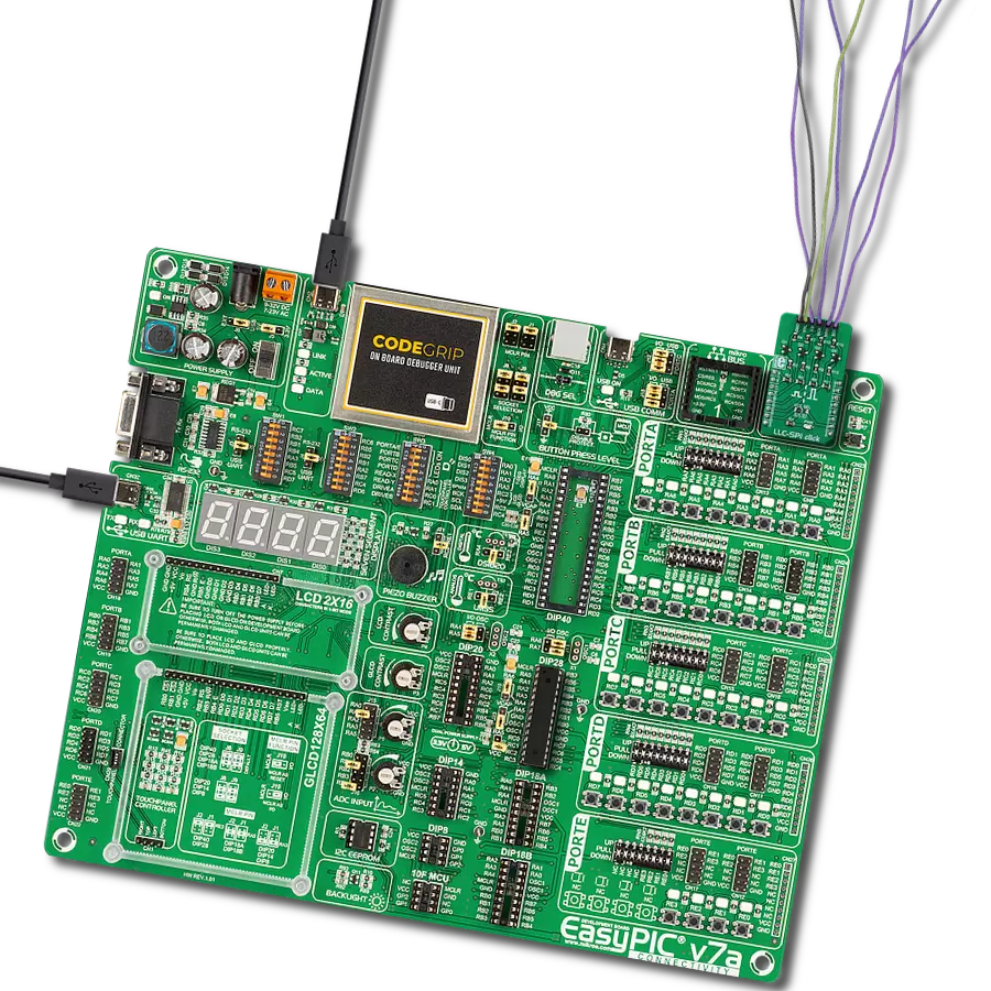
EasyPIC v7a
Compiler
NECTO Studio
MCU
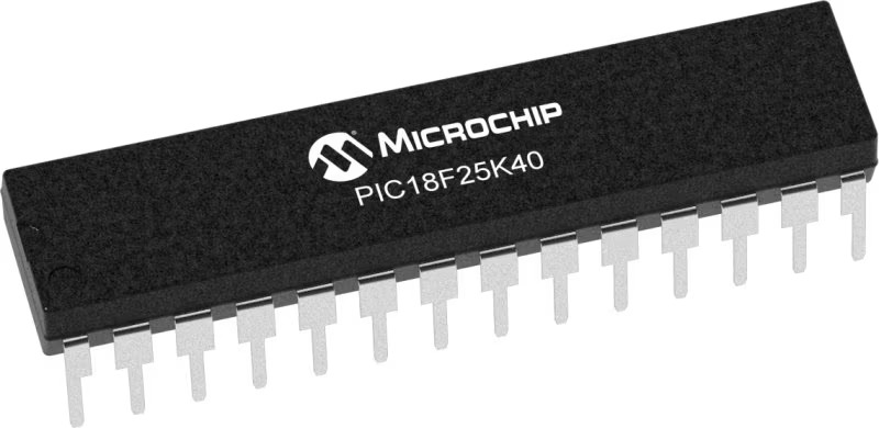
PIC18LF25K40
From concept to implementation, our SPI-signal logic level converter simplifies complex voltage conversion challenges, providing the precision, adaptability, and control you need to achieve exceptional results in your project
A
A
Hardware Overview
How does it work?
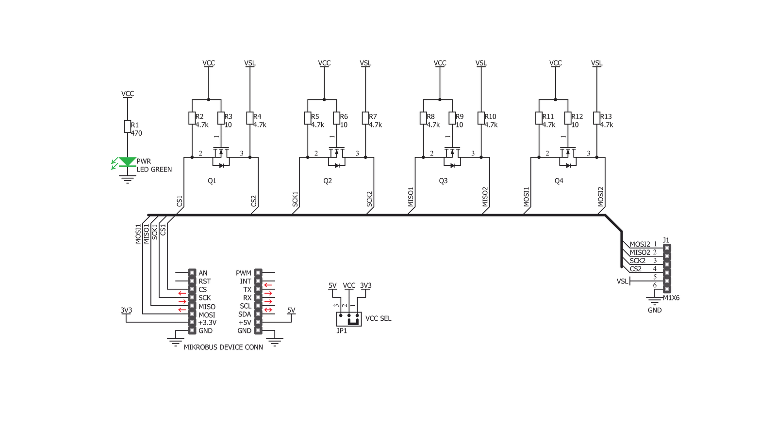
LLC SPI Click does not use any integrated circuit, as already mentioned. With ICs avoided completely, there are some benefits gained: the overall cost of the LLC circuit is greatly reduced, a more robust MOSFET solution reduces the failure rate, and when powered off, both the low voltage and the high voltage sides are isolated from one another (by non-conductive MOSFETs). This type of circuit is sometimes referred to as a level shifting or level translating circuit and it is often necessary when one SPI device (typically a sensor IC) uses different logic voltage levels for the communication than the controller device, which
is a microcontroller (MCU) in most cases. The conversion of this circuitry is bi-directional, which makes it suitable to be used with the SPI communication protocol. The SPI protocol was first introduced by Motorola, in the '80s. The circuit is divided into low-side and high-side sections for future reference, however, both up-shifting, and down-shifting of the voltage level is possible. The mechanisms are slightly different, so each will be explained separately. The reference voltage for the high-side can be selected by using the SMD jumper labeled as VCC SEL. The pull-up voltage for the high-side can be selected from the
mikroBUS™ power rails, so it can be either 3.3V or 5V. For the low-side, an arbitrary reference voltage can be applied to the VSL pin of the J1 header, respecting the maximum voltage rating, as well as the condition mentioned above. J1 is the standard, 2.54mm pin-header. The low-side SPI related pins are also routed to the J1 header, allowing an external device to be connected (using the standard wire-jumpers). As already mentioned, the low-side can actually use higher voltage levels than the master, but in most usage scenarios, it will be lower than the master, thus the terminology used in the text above.


Features overview
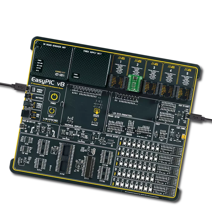
Development board
EasyPIC v7a is the seventh generation of PIC development boards specially designed for the needs of rapid development of embedded applications. It supports a wide range of 8-bit PIC microcontrollers from Microchip and has a broad set of unique functions, such as the first-ever embedded debugger/programmer over USB-C. The development board is well organized and designed so that the end-user has all the necessary elements in one place, such as switches, buttons, indicators, connectors, and others. With four different connectors for each port, EasyPIC v7a allows you to connect accessory boards, sensors, and custom electronics more efficiently than ever. Each part of the EasyPIC v7a development board
contains the components necessary for the most efficient operation of the same board. In addition to the advanced integrated CODEGRIP programmer/debugger module, which offers many valuable programming/debugging options and seamless integration with the Mikroe software environment, the board also includes a clean and regulated power supply module for the development board. It can use various external power sources, including an external 12V power supply, 7-23V AC or 9-32V DC via DC connector/screw terminals, and a power source via the USB Type-C (USB-C) connector. Communication options such as USB-UART and RS-232 are also included, alongside the well-
established mikroBUS™ standard, three display options (7-segment, graphical, and character-based LCD), and several different DIP sockets. These sockets cover a wide range of 8-bit PIC MCUs, from PIC10F, PIC12F, PIC16F, PIC16Enh, PIC18F, PIC18FJ, and PIC18FK families. EasyPIC v7a is an integral part of the Mikroe ecosystem for rapid development. Natively supported by Mikroe software tools, it covers many aspects of prototyping and development thanks to a considerable number of different Click boards™ (over a thousand boards), the number of which is growing every day.

Microcontroller Overview
MCU Card / MCU
Architecture
PIC
MCU Memory (KB)
32
Silicon Vendor
Microchip
Pin count
28
RAM (Bytes)
2048
Used MCU Pins
mikroBUS™ mapper
Take a closer look
Click board™ Schematic
Step by step
Project assembly

Start by selecting your development board and Click board™. Begin with the EasyPIC v7a as your development board.


Track your results in real time
Application Output
1. Application Output - In Debug mode, the 'Application Output' window enables real-time data monitoring, offering direct insight into execution results. Ensure proper data display by configuring the environment correctly using the provided tutorial.

2. UART Terminal - Use the UART Terminal to monitor data transmission via a USB to UART converter, allowing direct communication between the Click board™ and your development system. Configure the baud rate and other serial settings according to your project's requirements to ensure proper functionality. For step-by-step setup instructions, refer to the provided tutorial.

3. Plot Output - The Plot feature offers a powerful way to visualize real-time sensor data, enabling trend analysis, debugging, and comparison of multiple data points. To set it up correctly, follow the provided tutorial, which includes a step-by-step example of using the Plot feature to display Click board™ readings. To use the Plot feature in your code, use the function: plot(*insert_graph_name*, variable_name);. This is a general format, and it is up to the user to replace 'insert_graph_name' with the actual graph name and 'variable_name' with the parameter to be displayed.

Software Support
Library Description
This library contains API for LLC-SPI Click driver.
Key functions:
llcspi_generic_write- LLC SPI writellcspi_generic_read- LLC SPI readllcspi_generic_transfer- LLC SPI transfer
Open Source
Code example
The complete application code and a ready-to-use project are available through the NECTO Studio Package Manager for direct installation in the NECTO Studio. The application code can also be found on the MIKROE GitHub account.
/*!
* \file
* \brief llcspi Click example
*
* # Description
* This application is converter for logic signals.
*
* The demo application is composed of two sections :
*
* ## Application Init
* Initialization device init
*
* ## Application Task
* Counter passes through the loop and logs the value of the counter on the bargraph display
*
* *note:*
* Connection between BarGraph and LLC-SPI is made through SPI interface.
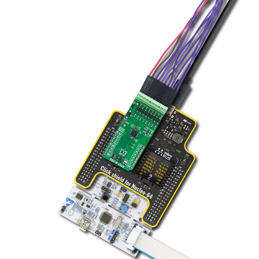
* You can connect a BarGraph Click to LLC-SPI Click with the wires to make connection between Click boards.
* We use the BarGraph Click to demonstrate the functions of the LLC-SPI Click.
*
* \author MikroE Team
*
*/
// ------------------------------------------------------------------- INCLUDES
#include "board.h"
#include "log.h"
#include "llcspi.h"
// ------------------------------------------------------------------ VARIABLES
static llcspi_t llcspi;
static log_t logger;
// ------------------------------------------------------ APPLICATION FUNCTIONS
void application_init ( void )
{
log_cfg_t log_cfg;
llcspi_cfg_t cfg;
/**
* Logger initialization.
* Default baud rate: 115200
* Default log level: LOG_LEVEL_DEBUG
* @note If USB_UART_RX and USB_UART_TX
* are defined as HAL_PIN_NC, you will
* need to define them manually for log to work.
* See @b LOG_MAP_USB_UART macro definition for detailed explanation.
*/
LOG_MAP_USB_UART( log_cfg );
log_init( &logger, &log_cfg );
log_info( &logger, "---- Application Init ----" );
// Click initialization.
llcspi_cfg_setup( &cfg );
LLCSPI_MAP_MIKROBUS( cfg, MIKROBUS_1 );
llcspi_init( &llcspi, &cfg );
}
void application_task ( void )
{
uint16_t convert;
uint8_t tmp[ 2 ];
uint8_t cnt;
// BarGraph display
for ( cnt = 0; cnt <= 10; cnt++ )
{
convert = ( uint16_t ) ( ( 1 << cnt ) - 1 );
tmp[ 1 ] = ( convert & 0x00FF );
tmp[ 0 ] = ( convert & 0xFF00 ) >> 8;
llcspi_generic_write( &llcspi, tmp, 2 );
Delay_ms ( 1000 );
}
}
int main ( void )
{
/* Do not remove this line or clock might not be set correctly. */
#ifdef PREINIT_SUPPORTED
preinit();
#endif
application_init( );
for ( ; ; )
{
application_task( );
}
return 0;
}
// ------------------------------------------------------------------------ END