Enhance your system performance with AD74412R and STM32F407VGT6
Compact yet powerful

Published Dec 29, 2023
Click board™
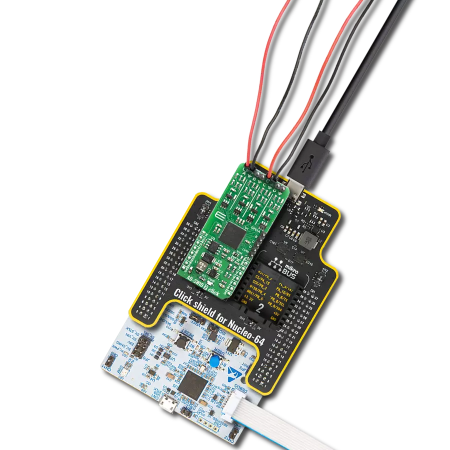
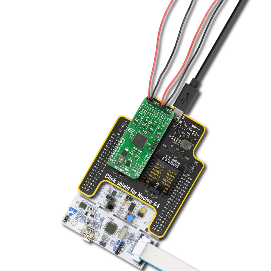
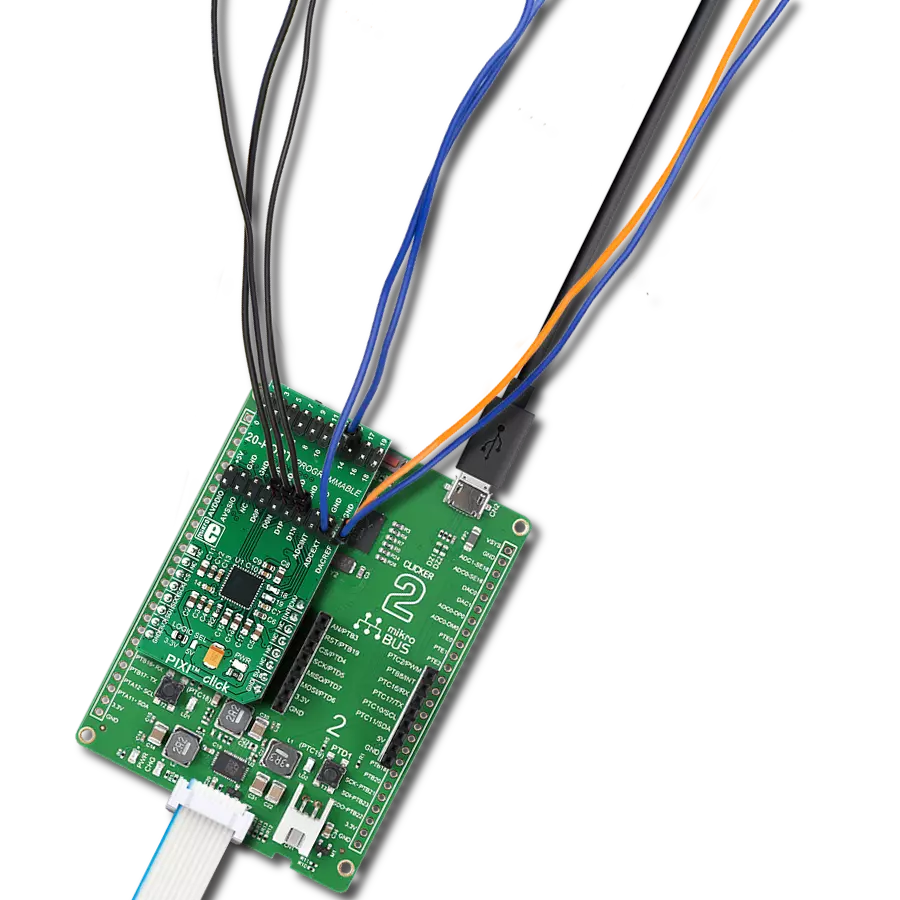
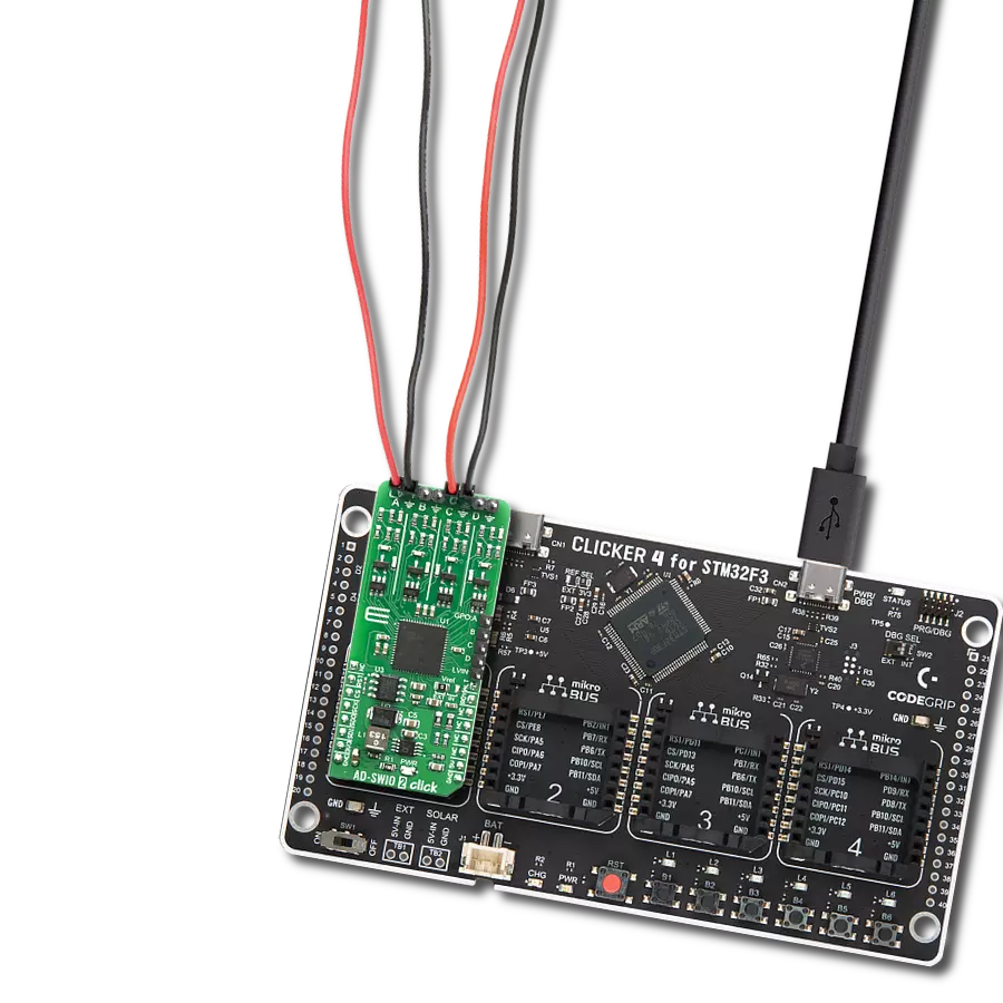
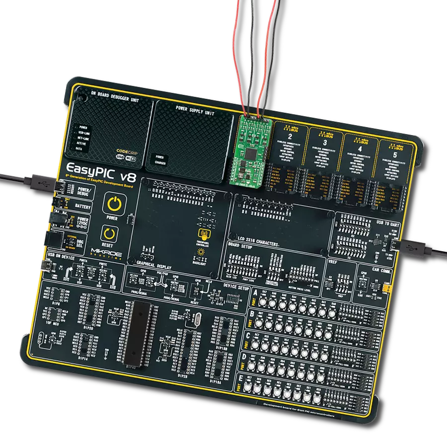
AD-SWIO Click
Dev. board
Clicker 4 for STM32F4
Compiler
NECTO Studio
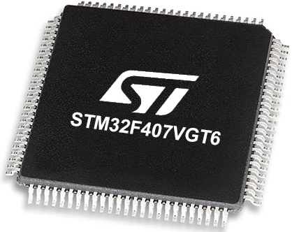
MCU
STM32F407VGT6
The game-changer for applications demanding simultaneous ADC and DAC functionality
A
A
Hardware Overview
How does it work?
AD-SWIO Click is based on AD74412R, a 16-bit analog-to-digital converter (ADC), and a 13-bit digital-to-analog converter (DAC) from Analog Devices. There are several modes related to the AD74412R. These modes are voltage output, current output, voltage input, externally powered current input, loop-powered current input, external RTD measurement, digital input logic, and loop-powered digital input. The ADC can measure the voltage across the 100Ω RSENSE or at each channel's I/OP_x screw terminal. In high impedance mode, the ADC, by default, measures the voltage across the screw terminals (I/OP_x to I/ON_x) in a 0V to 10V range. The ADC also provides diagnostic information on user-selectable inputs such as supplies, internal die temperature, reference, and regulators. The AD-SWIO Click has four GPO-x pins, one per channel (GPO-A, GPO-B, GPO-C, GPO-D).
Each channel GPO-x pin can be configured to the logic outputs of the digital input functions or a logic high or low output. The GPO-x pins can be set via the GPO_SELECT bits within the GPO_CONFIGx registers. The Click board™ also contains an LVIN ( Low Voltage Input) pin, the measurement voltage range on this pin is 0V to 2.5V. The AD74412R has four 13-bit DACs, one per channel. Each DAC core is a 13-bit string DAC. The architecture structure consists of a string of resistors, each with a value of R. The digital input code loaded to the DAC_CODEx registers determines which string node the voltage is tapped off from and fed into the output amplifier. This architecture is inherently monotonic and linear. The AD74412R has short-circuited limit in voltage output mode that is programmable per channel. The circuit minimizes glitching on the I/OP_x screw terminal when the AVDD
supply is ramping, or the use case configuration is changed. This short-circuit limit you can regulate with a positive analog supply on the AVDD pin, Output voltage on AD-SWIO 2 Click is limited to +20V. The AD-SWIO 2 Click is equipped with the ADP1613 step-up dc-to-dc switching converter from Analog Devices with an integrated power switch capable of providing an output voltage as high as 20V. This Click board™ can only be operated with a 3.3V logic voltage level. The board must perform appropriate logic voltage level conversion before using MCUs with different logic levels. However, the Click board™ comes equipped with a library containing functions and an example code that can be used as a reference for further development.

Features overview
Development board
Clicker 4 for STM32F4 is a compact development board designed as a complete solution that you can use to quickly build your own gadgets with unique functionalities. Featuring an STM32F407VGT6 MCU, four mikroBUS™ sockets for Click boards™ connectivity, power management, and more, it represents a perfect solution for the rapid development of many different types of applications. At its core is an STM32F407VGT6 MCU, a powerful microcontroller by STMicroelectronics based on the high-performance
Arm® Cortex®-M4 32-bit processor core operating at up to 168 MHz frequency. It provides sufficient processing power for the most demanding tasks, allowing Clicker 4 to adapt to any specific application requirements. Besides two 1x20 pin headers, four improved mikroBUS™ sockets represent the most distinctive connectivity feature, allowing access to a huge base of Click boards™, growing on a daily basis. Each section of Clicker 4 is clearly marked, offering an intuitive and clean interface. This makes working with the
development board much simpler and, thus, faster. The usability of Clicker 4 doesn’t end with its ability to accelerate the prototyping and application development stages: it is designed as a complete solution that can be implemented directly into any project, with no additional hardware modifications required. Four mounting holes [4.2mm/0.165”] at all four corners allow simple installation by using mounting screws.

Microcontroller Overview
MCU Card / MCU
Architecture
ARM Cortex-M4
MCU Memory (KB)
10
Silicon Vendor
STMicroelectronics
Pin count
100
RAM (Bytes)
100
Used MCU Pins
mikroBUS™ mapper
Take a closer look
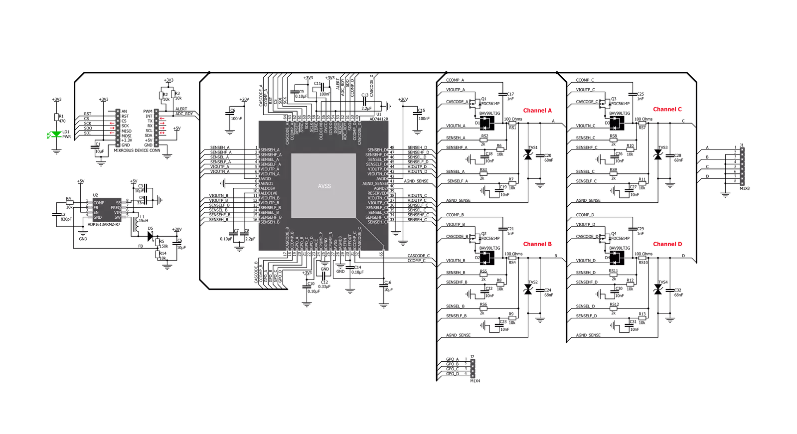
Click board™ Schematic
Step by step
Project assembly

Start by selecting your development board and Click board™. Begin with the Clicker 4 for STM32F4 as your development board.


Track your results in real time
Application Output
1. Application Output - In Debug mode, the 'Application Output' window enables real-time data monitoring, offering direct insight into execution results. Ensure proper data display by configuring the environment correctly using the provided tutorial.

2. UART Terminal - Use the UART Terminal to monitor data transmission via a USB to UART converter, allowing direct communication between the Click board™ and your development system. Configure the baud rate and other serial settings according to your project's requirements to ensure proper functionality. For step-by-step setup instructions, refer to the provided tutorial.

3. Plot Output - The Plot feature offers a powerful way to visualize real-time sensor data, enabling trend analysis, debugging, and comparison of multiple data points. To set it up correctly, follow the provided tutorial, which includes a step-by-step example of using the Plot feature to display Click board™ readings. To use the Plot feature in your code, use the function: plot(*insert_graph_name*, variable_name);. This is a general format, and it is up to the user to replace 'insert_graph_name' with the actual graph name and 'variable_name' with the parameter to be displayed.

Software Support
Library Description
This library contains API for AD-SWIO Click driver.
Key functions:
adswio_status_pin_ready- This function checks the status of the ready pin.adswio_get_conv_results- This function allows user to get the converted results of the selected channel.
Open Source
Code example
The complete application code and a ready-to-use project are available through the NECTO Studio Package Manager for direct installation in the NECTO Studio. The application code can also be found on the MIKROE GitHub account.
/*!
 * \file
 * \brief AdSwio Click example
 *
 * # Description
 * This Click provides a fully integrated single chip solution for input and output operation.
 * The AD-SWIO Click contains four 13-bit DACs, one per chanal, and 16-bit Σ-∆ ADC.
 * These options give a lot of flexibility in choosing functionality for analog output,
 * analog input, digital input, resistance temperature detector (RTD), and thermocouple
 * measurements integrated into a single chip solution with a serial peripheral interface (SPI).
 *
 * The demo application is composed of two sections :
 *
 * ## Application Init
 * Performs a hardware reset of the Click board and
 * executes a default configuration that enables channel A and sets it to measure voltage
 * input in the range from 0V to 10V, with 4800 SPS.
 *
 * ## Application Task
 * Waits for the data ready and then reads the results of ADC conversion from channel A
 * and if response is ok, then prints the results on the uart console.
 *
 * ## Additional Functions
 *
 * - void application_default_handler ( uint8_t *err_msg ) - Sends an error report messages from Click
 * driver to initialized console module. It must be set using adswio2_set_handler function.
 *
 *
 * \author MikroE Team
 *
 */
// ------------------------------------------------------------------- INCLUDES

#include "board.h"
#include "log.h"
#include "adswio.h"

// ------------------------------------------------------------------ VARIABLES

static adswio_t adswio;
static log_t logger;

static uint8_t adswio_rdy;
static adswio_err_t adswio_err;
static uint16_t adswio_ch_a;
static float adswio_res;

const uint16_t ADSWIO_RANGE_VOLT_MV = 10000;
const uint32_t ADSWIO_RANGE_RESOLUTION = 65536;

// ------------------------------------------------------ ADDITIONAL FUNCTIONS

void application_default_handler ( uint8_t *err_msg )
{
    char *err_ptr = err_msg;

    log_printf( &logger, "\r\n" );
    log_printf( &logger, "[ERROR] : %s", err_ptr );
    log_printf( &logger, "\r\n" );
}

// ------------------------------------------------------ APPLICATION FUNCTIONS

void application_init ( void )
{
    log_cfg_t log_cfg;
    adswio_cfg_t cfg;

    /**
     * Logger initialization.
     * Default baud rate: 115200
     * Default log level: LOG_LEVEL_DEBUG
     * @note If USB_UART_RX and USB_UART_TX
     * are defined as HAL_PIN_NC, you will
     * need to define them manually for log to work.
     * See @b LOG_MAP_USB_UART macro definition for detailed explanation.
     */
    LOG_MAP_USB_UART( log_cfg );
    log_init( &logger, &log_cfg );
    log_info( &logger, "---- Application Init ----" );

    //  Click initialization.

    adswio_cfg_setup( &cfg );
    ADSWIO_MAP_MIKROBUS( cfg, MIKROBUS_1 );
    adswio_init( &adswio, &cfg );
    Delay_ms ( 100 );

    adswio_default_cfg( &adswio );
    Delay_ms ( 1000 );

    adswio_rdy  = DUMMY;
    adswio_ch_a = DUMMY;
    adswio_res  = DUMMY;
    adswio_err  = ADSWIO_ERR_STATUS_OK;

    log_printf( &logger, " AD-SWIO Click initialization done \r\n");
    log_printf( &logger, "************************************\r\n");
}

void application_task ( void )
{
    uint16_t timeout = 0;
    do
    {
        Delay_1ms( );
        timeout++;
        adswio_rdy = adswio_status_pin_ready( &adswio );
        if ( timeout > 3000 )
        {
            timeout = 0;
            log_printf( &logger, " Reinitializing...");
            adswio_default_cfg( &adswio );
            log_printf( &logger, "Done\r\n");
        }
    }
    while ( adswio_rdy != 0 );

    adswio_err = adswio_get_conv_results( &adswio, ADSWIO_SETUP_CONV_EN_CHA, &adswio_ch_a );

    if ( adswio_err == ADSWIO_ERR_STATUS_OK )
    {
        adswio_res = adswio_ch_a;
        adswio_res /= ADSWIO_RANGE_RESOLUTION;
        adswio_res *= ADSWIO_RANGE_VOLT_MV;
        adswio_ch_a = adswio_res;

        log_printf( &logger, " Voltage from channel A: %d mV\r\n", adswio_ch_a );

        log_printf( &logger, "-----------------------------------\r\n\r\n" );
        Delay_ms ( 200 );
    }
}

int main ( void )
{
    /* Do not remove this line or clock might not be set correctly. */
    #ifdef PREINIT_SUPPORTED
    preinit();
    #endif

    application_init( );

    for ( ; ; )
    {
        application_task( );
    }

    return 0;
}


// ------------------------------------------------------------------------ END
Additional Support
Resources
Category:ADC-DAC