Deliver precise electrical isolation and signal conditioning with DCL540C01 and PIC18F57Q43
Explore the future of industrial automation and beyond.

Published Feb 13, 2024
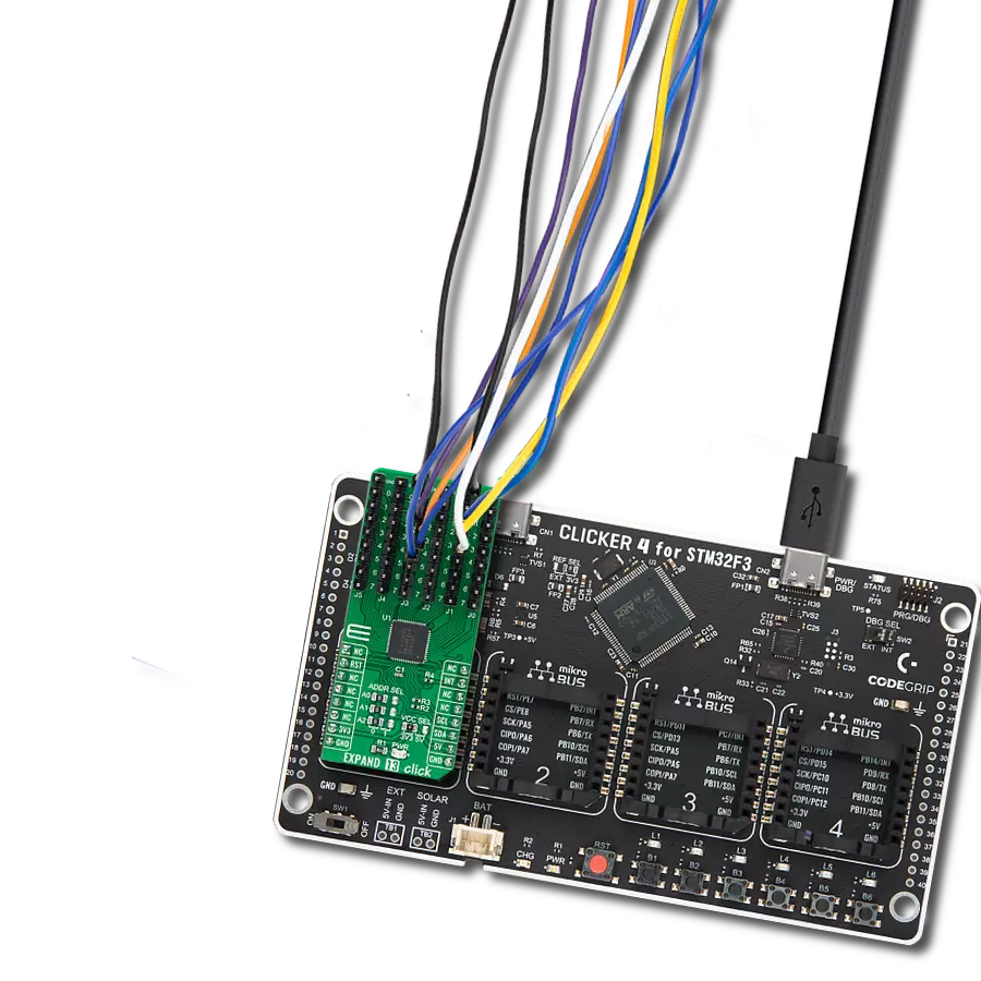
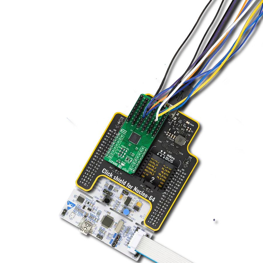
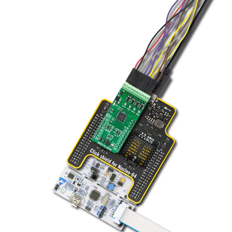
Click board™
DIGI Isolator Click
Dev. board
Curiosity Nano with PIC18F57Q43
Compiler
NECTO Studio
MCU
PIC18F57Q43
Perfect solution for developers pushing the boundaries in industrial automation, motor control, inverters, and more. Experience enhanced SPI and UART interface isolation where it matters.
A
A
Hardware Overview
How does it work?
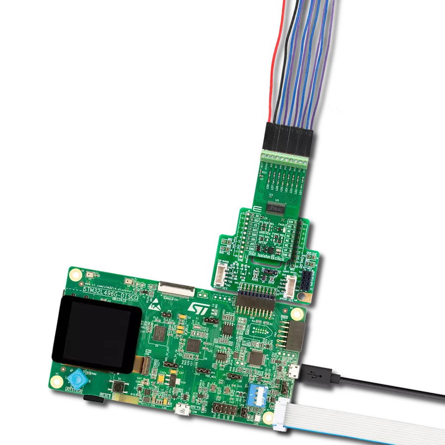
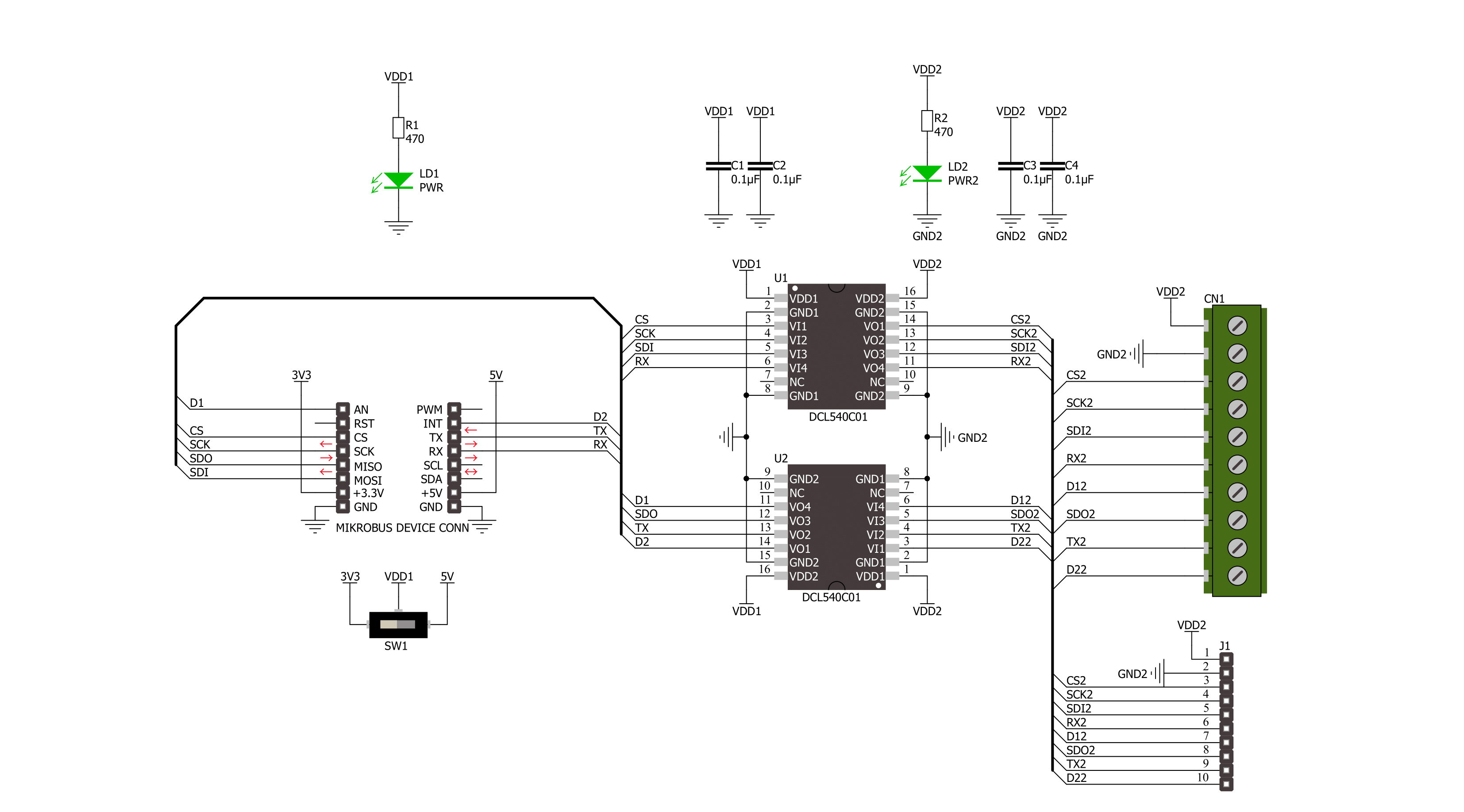
DIGI Isolator Click is based on two DCL540C01, high-speed, quad-channel digital isolators from Toshiba Semiconductor. Toshiba used the magnetic coupling structure and CMOS technology to achieve high reinforced isolation. The isolated lines are divided into two electrically connected groups. The first group comes in the form of 8 screw terminals, while the second forms a classic male 10-header row for easier jumper wire usage. Both groups of connectors have the same functions and are labeled the same. You can
distinguish the power VDD2 and GND2 lines from the data lines: four SPI, UART TX/RX, and two digital IO lines. The isolator can work with supply voltages from 2.25 up to 5.5V. DIGI Isolator Click uses standard 4-Wire SPI serial interface lines, standard UART TX/RX interface lines, and two additional GP lines from the mikroBUS™ socket as an insulated extension, marked D2 and D1, respectively. The SPI and UART pins are labeled according to the standard interface markings. These eight lines go through the DCL540C01s to
the terminals and headers, thus isolating the host MCU from the connected device. This Click board™ can operate with either 3.3V or 5V logic voltage levels selected via the VCC SEL switch. This way, both 3.3V and 5V capable MCUs can use the communication lines properly. Also, this Click board™ comes equipped with a library containing easy-to-use functions and an example code that can be used as a reference for further development.

Features overview
Development board
PIC18F57Q43 Curiosity Nano evaluation kit is a cutting-edge hardware platform designed to evaluate microcontrollers within the PIC18-Q43 family. Central to its design is the inclusion of the powerful PIC18F57Q43 microcontroller (MCU), offering advanced functionalities and robust performance. Key features of this evaluation kit include a yellow user LED and a responsive
mechanical user switch, providing seamless interaction and testing. The provision for a 32.768kHz crystal footprint ensures precision timing capabilities. With an onboard debugger boasting a green power and status LED, programming and debugging become intuitive and efficient. Further enhancing its utility is the Virtual serial port (CDC) and a debug GPIO channel (DGI
GPIO), offering extensive connectivity options. Powered via USB, this kit boasts an adjustable target voltage feature facilitated by the MIC5353 LDO regulator, ensuring stable operation with an output voltage ranging from 1.8V to 5.1V, with a maximum output current of 500mA, subject to ambient temperature and voltage constraints.

Microcontroller Overview
MCU Card / MCU

Architecture
PIC
MCU Memory (KB)
128
Silicon Vendor
Microchip
Pin count
48
RAM (Bytes)
8196
You complete me!
Accessories
Curiosity Nano Base for Click boards is a versatile hardware extension platform created to streamline the integration between Curiosity Nano kits and extension boards, tailored explicitly for the mikroBUS™-standardized Click boards and Xplained Pro extension boards. This innovative base board (shield) offers seamless connectivity and expansion possibilities, simplifying experimentation and development. Key features include USB power compatibility from the Curiosity Nano kit, alongside an alternative external power input option for enhanced flexibility. The onboard Li-Ion/LiPo charger and management circuit ensure smooth operation for battery-powered applications, simplifying usage and management. Moreover, the base incorporates a fixed 3.3V PSU dedicated to target and mikroBUS™ power rails, alongside a fixed 5.0V boost converter catering to 5V power rails of mikroBUS™ sockets, providing stable power delivery for various connected devices.

Used MCU Pins
mikroBUS™ mapper
Take a closer look
Click board™ Schematic
Step by step
Project assembly

Start by selecting your development board and Click board™. Begin with the Curiosity Nano with PIC18F57Q43 as your development board.


Track your results in real time
Application Output
1. Application Output - In Debug mode, the 'Application Output' window enables real-time data monitoring, offering direct insight into execution results. Ensure proper data display by configuring the environment correctly using the provided tutorial.

2. UART Terminal - Use the UART Terminal to monitor data transmission via a USB to UART converter, allowing direct communication between the Click board™ and your development system. Configure the baud rate and other serial settings according to your project's requirements to ensure proper functionality. For step-by-step setup instructions, refer to the provided tutorial.

3. Plot Output - The Plot feature offers a powerful way to visualize real-time sensor data, enabling trend analysis, debugging, and comparison of multiple data points. To set it up correctly, follow the provided tutorial, which includes a step-by-step example of using the Plot feature to display Click board™ readings. To use the Plot feature in your code, use the function: plot(*insert_graph_name*, variable_name);. This is a general format, and it is up to the user to replace 'insert_graph_name' with the actual graph name and 'variable_name' with the parameter to be displayed.

Software Support
Library Description
This library contains API for DIGI Isolator Click driver.
Key functions:
digiisolator_spi_transfer- DIGI Isolator SPI transfer function.digiisolator_uart_write- DIGI Isolator UART data writing functiondigiisolator_get_d1_pin_voltage- DIGI Isolator read D1 pin voltage level function.
Open Source
Code example
The complete application code and a ready-to-use project are available through the NECTO Studio Package Manager for direct installation in the NECTO Studio. The application code can also be found on the MIKROE GitHub account.
/*!
 * @file main.c
 * @brief DIGI Isolator Click example
 *
 * # Description
 * This example demonstrates the use of the DIGI Isolator Click board
 * by reading and writing data by using SPI and UART serial interface
 * and reading results of AD conversion.
 *
 * The demo application is composed of two sections :
 *
 * ## Application Init
 * Initialization of SPI, UART and ADC module and log UART.
 *
 * ## Application Task
 * At the start, the demo application reads and checks the manufacturer ID and
 * device ID of the connected Flash 11 Click board by using SPI serial interface.
 * After that, sends a "MikroE" message, reads the received data,
 * and parses it by using UART serial interface in loopback mode.
 * And finally, the demo app reads the results of the AD conversion of the D1 (AN) pin.
 * Results are being sent to the UART Terminal, where you can track their changes.
 *
 * @author Nenad Filipovic
 *
 */

#include "board.h"
#include "log.h"
#include "digiisolator.h"

#define FLASH11_CMD_GET_ID         0x90, 0x00, 0x00, 0x00, 0x00, 0x00
#define FLASH11_MANUFACTURER_ID    0x1F
#define FLASH11_DEVICE_ID          0x15
#define DEMO_MESSAGE               "\r\nMikroE\r\n"
#define PROCESS_BUFFER_SIZE        200

static digiisolator_t digiisolator;
static log_t logger;

void application_init ( void )
{
    log_cfg_t log_cfg;  /**< Logger config object. */
    digiisolator_cfg_t digiisolator_cfg;  /**< Click config object. */

    /**
     * Logger initialization.
     * Default baud rate: 115200
     * Default log level: LOG_LEVEL_DEBUG
     * @note If USB_UART_RX and USB_UART_TX
     * are defined as HAL_PIN_NC, you will
     * need to define them manually for log to work.
     * See @b LOG_MAP_USB_UART macro definition for detailed explanation.
     */
    LOG_MAP_USB_UART( log_cfg );
    log_init( &logger, &log_cfg );
    log_info( &logger, " Application Init " );

    // Click initialization.
    digiisolator_cfg_setup( &digiisolator_cfg );
    DIGIISOLATOR_MAP_MIKROBUS( digiisolator_cfg, MIKROBUS_1 );
    if ( SPI_MASTER_ERROR == digiisolator_init( &digiisolator, &digiisolator_cfg ) )
    {
        log_error( &logger, " Communication init." );
        for ( ; ; );
    }

    log_info( &logger, " Application Task " );
    log_printf( &logger, " -----------------------\r\n" );
    Delay_ms ( 100 );
}

void application_task ( void )
{
    static uint8_t cmd_get_id[ 6 ] = { FLASH11_CMD_GET_ID };
    static uint8_t read_id[ 6 ] = { 0 };
    static char app_buf[ PROCESS_BUFFER_SIZE ] = { 0 };
    static float voltage = 0;

    if ( DIGIISOLATOR_OK == digiisolator_spi_transfer( &digiisolator, &cmd_get_id[ 0 ], &read_id[ 0 ], 6 ) )
    {
        if ( ( FLASH11_MANUFACTURER_ID == read_id[ 4 ] ) && ( FLASH11_DEVICE_ID == read_id[ 5 ] ) )
        {
            log_printf( &logger, " SPI\r\n" );
            log_printf( &logger, " Manufacturer ID: 0x%.2X\r\n", ( uint16_t ) read_id[ 4 ] );
            log_printf( &logger, " Device ID: 0x%.2X    \r\n", ( uint16_t ) read_id[ 5 ] );
            log_printf( &logger, " -----------------------\r\n" );
            Delay_ms ( 1000 );
            Delay_ms ( 1000 );
        }
    }

    if ( 0 < digiisolator_uart_write( &digiisolator, DEMO_MESSAGE, strlen( DEMO_MESSAGE ) ) )
    {
        if ( 0 < digiisolator_uart_read( &digiisolator, app_buf, strlen( DEMO_MESSAGE ) ) )
        {
            log_printf( &logger, " UART\r\n" );
            log_printf( &logger, "%s", app_buf );
            memset( app_buf, 0, PROCESS_BUFFER_SIZE );
            log_printf( &logger, " -----------------------\r\n" );
            Delay_ms ( 1000 );
            Delay_ms ( 1000 );
        }
    }

    if ( DIGIISOLATOR_OK == digiisolator_get_d1_pin_voltage ( &digiisolator, &voltage ) )
    {
        log_printf( &logger, " ADC\r\n" );
        log_printf( &logger, " Voltage : %.3f[V]\r\n", voltage );
        log_printf( &logger, " -----------------------\r\n" );
        Delay_ms ( 1000 );
        Delay_ms ( 1000 );
    }
}

int main ( void )
{
    /* Do not remove this line or clock might not be set correctly. */
    #ifdef PREINIT_SUPPORTED
    preinit();
    #endif

    application_init( );

    for ( ; ; )
    {
        application_task( );
    }

    return 0;
}

// ------------------------------------------------------------------------ END
Additional Support
Resources
Category:Port expander