Adjust and optimize critical settings in your projects with 67WR100KLF and PIC18F47K42TQFP
Trim with precision: Elevate control with our trimmer potentiometer

Published Feb 13, 2024
Click board™
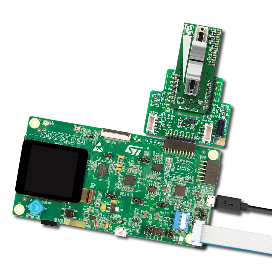
POT 2 Click
Dev. board
Curiosity Nano with PIC18F47K42
Compiler
NECTO Studio
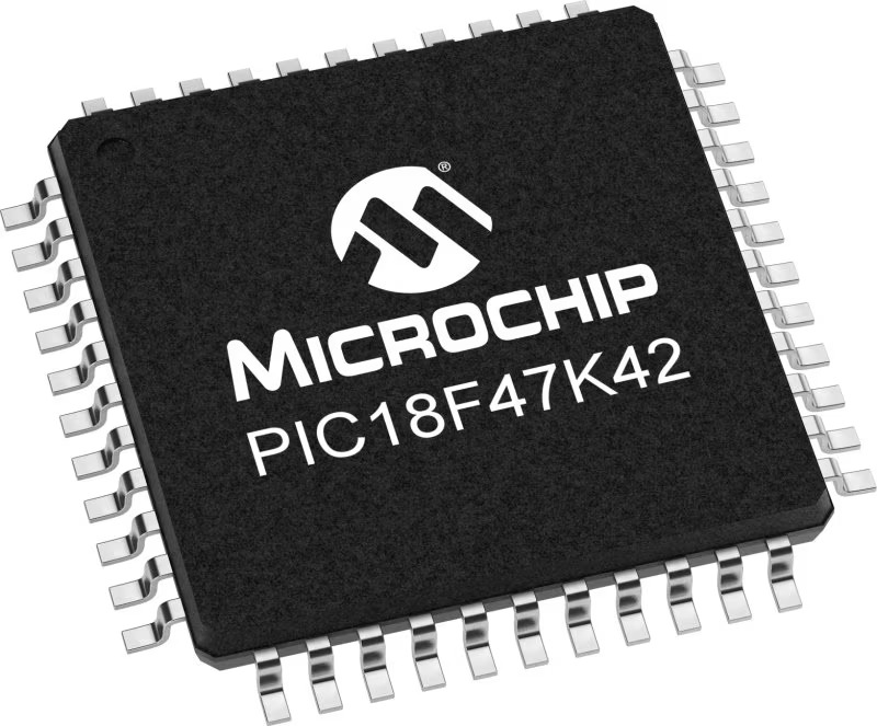
MCU
PIC18F47K42TQFP
Our trimmer potentiometers are meticulously crafted to deliver unparalleled precision, enabling you to calibrate and fine-tune your equipment with exceptional accuracy, so you can achieve peak performance effortlessly
A
A
Hardware Overview
How does it work?
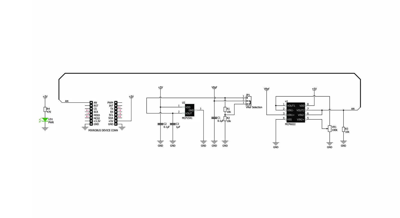
POT 2 Click is based on the MCP1541, a precision voltage reference IC from Microchip is used to provide the voltage of 4.096V. is fed to an input of an operational amplifier, that acts as the buffer, with the unity gain. The output of the first buffer is fed to one end of a high-precision trimmer-potentiometer. The second end of the potentiometer is grounded, while the middle tap of the potentiometer is used as the input to a second buffer. The output of the second buffer is routed to the AN pin of the mikroBUS™, allowing the host microcontroller (MCU) to use the output voltage for any purpose. The design uses the MCP6022, a dual, rail-to-rail operational amplifier from Microchip. This operational amplifier is a perfect choice for this design, as it allows rail-to-rail
operation, uses a single power supply of 5V, and has a stable unity gain. Without the buffers, the variable impedance would affect the reference voltage. The reference voltage IC can provide less than 10 mA, with the significant voltage drop for output currents exceeding 2 mA. Therefore, the MCP6022 used as a dual buffer ensures good stability of the circuit. The potentiometer itself is a multi-turn type of potentiometer which provides high accuracy. It is equipped with a screw, which can be rotated 20 times between the end positions. This allows the resistance to be precisely selected. The fact that the screw fits tightly into the casing of the potentiometer, ensures that no resistance variations are possible, unlike the conventional knob or slider potentiometers.
POT 2 click is equipped with the SMD jumper, which is used to select the voltage reference for the potentiometer. There are two options available: 2.048V and 4.096V. These values are the most commonly used voltage references for different kinds of A/D converters. Most MCUs which use 3.3V for the power supply, do not have the option to use 4.096V (full voltage output of the MCP1541 IC), so an option to select 2.048V by dividing the output voltage of the MCP1541 IC, is very useful in that case. The voltage reference can be selected by moving the SMD jumper labeled as VRef SEL to the desired position (2.048V or 4.096V).


Features overview
Development board
PIC18F47K42 Curiosity Nano evaluation kit is a cutting-edge hardware platform designed to evaluate the PIC18F47K42 microcontroller (MCU). Central to its design is the inclusion of the powerful PIC18F47K42 microcontroller (MCU), offering advanced functionalities and robust performance. Key features of this evaluation kit include a yellow user LED and a responsive mechanical user switch
providing seamless interaction and testing. The provision for a 32.768kHz crystal footprint ensures precision timing capabilities. With an onboard debugger boasting a green power and status LED, programming and debugging become intuitive and efficient. Further enhancing its utility is the Virtual serial port (CDC) and a debug GPIO channel (DGI GPIO), offering extensive connectivity options.
Powered via USB, this kit boasts an adjustable target voltage feature facilitated by the MIC5353 LDO regulator, ensuring stable operation with an output voltage ranging from 2.3V to 5.1V (limited by USB input voltage), with a maximum output current of 500mA, subject to ambient temperature and voltage constraints.

Microcontroller Overview
MCU Card / MCU
Architecture
PIC
MCU Memory (KB)
128
Silicon Vendor
Microchip
Pin count
40
RAM (Bytes)
8192
You complete me!
Accessories
Curiosity Nano Base for Click boards is a versatile hardware extension platform created to streamline the integration between Curiosity Nano kits and extension boards, tailored explicitly for the mikroBUS™-standardized Click boards and Xplained Pro extension boards. This innovative base board (shield) offers seamless connectivity and expansion possibilities, simplifying experimentation and development. Key features include USB power compatibility from the Curiosity Nano kit, alongside an alternative external power input option for enhanced flexibility. The onboard Li-Ion/LiPo charger and management circuit ensure smooth operation for battery-powered applications, simplifying usage and management. Moreover, the base incorporates a fixed 3.3V PSU dedicated to target and mikroBUS™ power rails, alongside a fixed 5.0V boost converter catering to 5V power rails of mikroBUS™ sockets, providing stable power delivery for various connected devices.

Used MCU Pins
mikroBUS™ mapper
Take a closer look
Click board™ Schematic
Step by step
Project assembly
Start by selecting your development board and Click board™. Begin with the Curiosity Nano with PIC18F47K42 as your development board.


Track your results in real time
Application Output
1. Application Output - In Debug mode, the 'Application Output' window enables real-time data monitoring, offering direct insight into execution results. Ensure proper data display by configuring the environment correctly using the provided tutorial.

2. UART Terminal - Use the UART Terminal to monitor data transmission via a USB to UART converter, allowing direct communication between the Click board™ and your development system. Configure the baud rate and other serial settings according to your project's requirements to ensure proper functionality. For step-by-step setup instructions, refer to the provided tutorial.

3. Plot Output - The Plot feature offers a powerful way to visualize real-time sensor data, enabling trend analysis, debugging, and comparison of multiple data points. To set it up correctly, follow the provided tutorial, which includes a step-by-step example of using the Plot feature to display Click board™ readings. To use the Plot feature in your code, use the function: plot(*insert_graph_name*, variable_name);. This is a general format, and it is up to the user to replace 'insert_graph_name' with the actual graph name and 'variable_name' with the parameter to be displayed.

Software Support
Library Description
This library contains API for POT 2 Click driver.
Key functions:
pot2_generic_read- Generic read function
Open Source
Code example
The complete application code and a ready-to-use project are available through the NECTO Studio Package Manager for direct installation in the NECTO Studio. The application code can also be found on the MIKROE GitHub account.
/*!
 * \file
 * \brief Pot2 Click example
 *
 * # Description
 * This demo-app shows the ADC values using POT 2 Click board.
 *
 * The demo application is composed of two sections :
 *
 * ## Application Init
 * Configures Clicks and log objects.
 *
 * ## Application Task
 * Demo app reads ADC data and displays them as dec and hex values every second
 *
 * \author Jovan Stajkovic
 *
 */
// ------------------------------------------------------------------- INCLUDES

#include "board.h"
#include "log.h"
#include "pot2.h"

// ------------------------------------------------------------------ VARIABLES

static pot2_t pot2;
static log_t logger;

static uint16_t adc_val;
static float voltage_val;

// ------------------------------------------------------ APPLICATION FUNCTIONS

void application_init ( void )
{
    log_cfg_t log_cfg;
    pot2_cfg_t cfg;

    /**
     * Logger initialization.
     * Default baud rate: 115200
     * Default log level: LOG_LEVEL_DEBUG
     * @note If USB_UART_RX and USB_UART_TX
     * are defined as HAL_PIN_NC, you will
     * need to define them manually for log to work.
     * See @b LOG_MAP_USB_UART macro definition for detailed explanation.
     */
    LOG_MAP_USB_UART( log_cfg );
    log_init( &logger, &log_cfg );
    log_info( &logger, "---- Application Init ----" );

    //  Click initialization.

    pot2_cfg_setup( &cfg );
    POT2_MAP_MIKROBUS( cfg, MIKROBUS_1 );
    if ( pot2_init( &pot2, &cfg ) == ADC_ERROR )
    {
        log_info( &logger, "---- Application Init Error ----" );
        log_info( &logger, "---- Please, run program again ----" );

        for ( ; ; );
    }
    log_info( &logger, "---- Application Init Done ----\r\n" );

    voltage_val = 0;
    adc_val = 0;
}

void application_task ( void )
{
    if ( pot2_read_adc ( &pot2, &adc_val ) != ADC_ERROR )
    {
        log_printf( &logger, " ADC value : [DEC] %u, [HEX] 0x%x\r\n", adc_val, adc_val );
    }

    if ( pot2_read_pin_voltage ( &pot2, &voltage_val ) != ADC_ERROR )
    {
        log_printf( &logger, " Voltage value : %.2f\r\n", voltage_val );
    }

    log_printf( &logger, "------------------------------------------\r\n" );
    Delay_ms ( 1000 );
}

int main ( void )
{
    /* Do not remove this line or clock might not be set correctly. */
    #ifdef PREINIT_SUPPORTED
    preinit();
    #endif

    application_init( );

    for ( ; ; )
    {
        application_task( );
    }

    return 0;
}


// ------------------------------------------------------------------------ END
Additional Support
Resources
Category:Potentiometers