Enhance access control and security measures with PN5180A0HN and ATmega328P
Your world, just a touch away: Embrace the NFC experience

Published Feb 14, 2024
Click board™
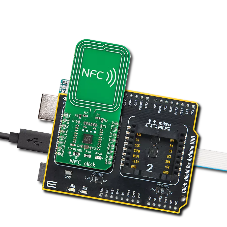
NFC 3 Click
Dev. board
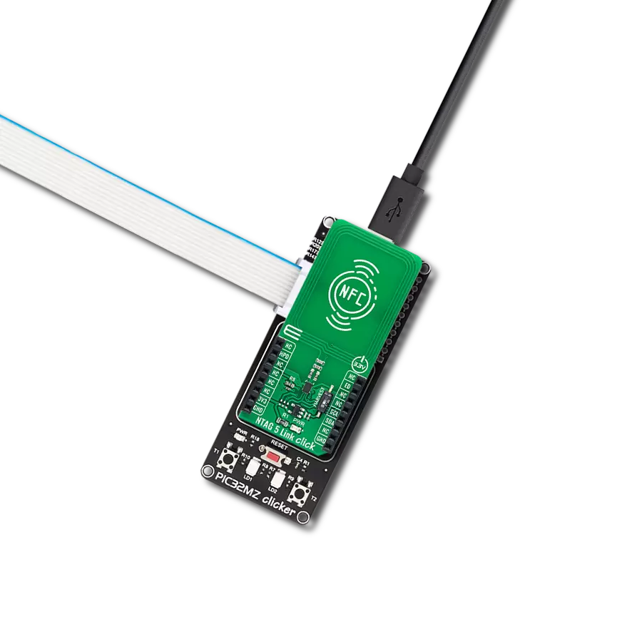
Arduino UNO Rev3
Compiler
NECTO Studio
MCU
ATmega328P
Step into a future where NFC simplifies and enhances your daily life, offering the convenience of secure payments and instant data sharing
A
A
Hardware Overview
How does it work?
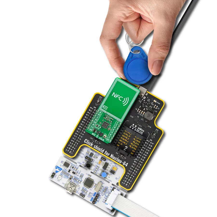
NFC 3 Click is based on the PN5180A0HN, a high-performance multiprotocol full NFC frontend from NXP Semiconductors, for contactless communication at 13.56MHz. The PN5180A0HN implements the RF and all the low-level functionality, like an antenna driving and receiver circuitry, to realize an NFC Forum-compliant reader. It utilizes an outstanding modulation and demodulation concept for different contactless communication methods and protocols. The PN5180A0HN is fully compliant with many Reader/Writer standards like ISO 14443A/B up to 848 kBit/s, JIS X 6319-4 comparable with FeliCa scheme, ISO 15693, ISO 18092, and more. Alongside support for reading all NFC tag types (type 1, 2, 3, 4A, and 4B) and high RF output power, this Click board™ is ideally suited for industrial and consumer NFC applications like industrial, eGov readers, payment terminals, and more. This Click board™ connects to a host MCU with an SPI
interface for configuration, NFC data exchange, and high-level NFC protocol implementation. It supports the most common SPI Mode 0 and operates with data rates up to 7 Mbit/s. The PN5180A0HN has two types of integrated memories: RAM and EEPROM. Internal registers of the PN5180A0HN store configuration data, while the RF configuration for dedicated RF protocols is defined by EEPROM data, copied by a command issued from the host MCU. This allows users to achieve maximum RF performance from a given antenna design. In addition to the SPI interface signals, this board uses several other signals from the mikroBUS™ socket. The reset pin routed on the RST pin of the mikroBUS™ socket provides the general reset ability, while the IRQ pin of the mikroBUS™ socket represents an interrupt request to inform the host controller of various events. The PN5180A0HN also has the possibility of updating the implemented firmware. In Secure
Firmware update mode, the PN5180A0HN requires dedicated physical handling of the SPI interface lines and the BSY line of the mikroBUS™ socket. The BSY signal is used to indicate that the PN5180A0HN is not able to send or receive data over the SPI interface. The secure firmware download mode is entered by setting the AUX pin to a high logic state during the Start-Up sequence of the device. The AUX pin is allowed for any other functionality after Start-Up (as test signals provided by test points on the board); the level of this pin has no impact on the download functionality after Start-Up during standard NFC operation. This Click board™ can be operated only with a 3.3V logic voltage level. The board must perform appropriate logic voltage level conversion before using MCUs with different logic levels. Also, it comes equipped with a library containing functions and an example code that can be used as a reference for further development.


Features overview
Development board
Arduino UNO is a versatile microcontroller board built around the ATmega328P chip. It offers extensive connectivity options for various projects, featuring 14 digital input/output pins, six of which are PWM-capable, along with six analog inputs. Its core components include a 16MHz ceramic resonator, a USB connection, a power jack, an
ICSP header, and a reset button, providing everything necessary to power and program the board. The Uno is ready to go, whether connected to a computer via USB or powered by an AC-to-DC adapter or battery. As the first USB Arduino board, it serves as the benchmark for the Arduino platform, with "Uno" symbolizing its status as the
first in a series. This name choice, meaning "one" in Italian, commemorates the launch of Arduino Software (IDE) 1.0. Initially introduced alongside version 1.0 of the Arduino Software (IDE), the Uno has since become the foundational model for subsequent Arduino releases, embodying the platform's evolution.

Microcontroller Overview
MCU Card / MCU

Architecture
AVR
MCU Memory (KB)
32
Silicon Vendor
Microchip
Pin count
28
RAM (Bytes)
2048
You complete me!
Accessories
Click Shield for Arduino UNO has two proprietary mikroBUS™ sockets, allowing all the Click board™ devices to be interfaced with the Arduino UNO board without effort. The Arduino Uno, a microcontroller board based on the ATmega328P, provides an affordable and flexible way for users to try out new concepts and build prototypes with the ATmega328P microcontroller from various combinations of performance, power consumption, and features. The Arduino Uno has 14 digital input/output pins (of which six can be used as PWM outputs), six analog inputs, a 16 MHz ceramic resonator (CSTCE16M0V53-R0), a USB connection, a power jack, an ICSP header, and reset button. Most of the ATmega328P microcontroller pins are brought to the IO pins on the left and right edge of the board, which are then connected to two existing mikroBUS™ sockets. This Click Shield also has several switches that perform functions such as selecting the logic levels of analog signals on mikroBUS™ sockets and selecting logic voltage levels of the mikroBUS™ sockets themselves. Besides, the user is offered the possibility of using any Click board™ with the help of existing bidirectional level-shifting voltage translators, regardless of whether the Click board™ operates at a 3.3V or 5V logic voltage level. Once you connect the Arduino UNO board with our Click Shield for Arduino UNO, you can access hundreds of Click boards™, working with 3.3V or 5V logic voltage levels.

Used MCU Pins
mikroBUS™ mapper
Take a closer look
Click board™ Schematic

Step by step
Project assembly

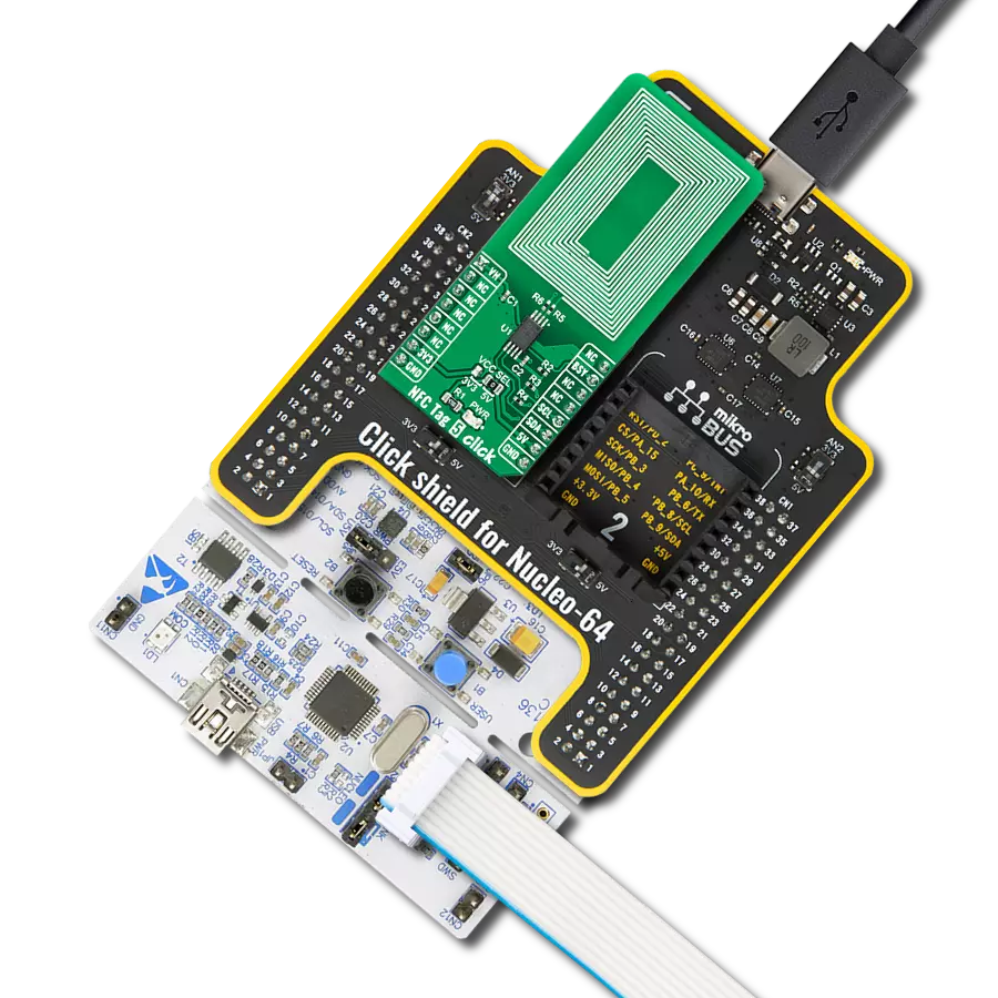
Start by selecting your development board and Click board™. Begin with the Arduino UNO Rev3 as your development board.


Software Support
Library Description
This library contains API for NFC 3 Click driver.
Key functions:
nfc3_read_card_uid- NFC 3 read card UID function.nfc3_read_firmware_version- NFC 3 reading firmware version function.nfc3_read_eeprom_version- NFC 3 reading EEPROM version function.
Open Source
Code example
The complete application code and a ready-to-use project are available through the NECTO Studio Package Manager for direct installation in the NECTO Studio. The application code can also be found on the MIKROE GitHub account.
/*!
 * @file main.c
 * @brief NFC3 Click example
 *
 * # Description
 * This example demonstrates the use of NFC 3 Click board
 * by reading MIFARE ISO/IEC 14443 type A tag UID.
 *
 * The demo application is composed of two sections :
 *
 * ## Application Init
 * Initializes driver and logger, then enables the Click board and reads
 * the device product, firmware and eeprom versions.
 *
 * ## Application Task
 * If there's a tag detected, it reads its UID and displays it on USB UART.
 *
 * @note
 * Only tags with 4-byte or 7-byte UIDs are compatible with this example.
 * We recommend MIKROE-1475 - an RFiD tag 13.56MHz compliant with ISO14443-A standard.
 *
 * @author Stefan Filipovic
 *
 */

#include "board.h"
#include "log.h"
#include "nfc3.h"

static nfc3_t nfc3;
static log_t logger;
static uint16_t info;

void application_init ( void )
{
    log_cfg_t log_cfg;  /**< Logger config object. */
    nfc3_cfg_t nfc3_cfg;  /**< Click config object. */

    /**
     * Logger initialization.
     * Default baud rate: 115200
     * Default log level: LOG_LEVEL_DEBUG
     * @note If USB_UART_RX and USB_UART_TX
     * are defined as HAL_PIN_NC, you will
     * need to define them manually for log to work.
     * See @b LOG_MAP_USB_UART macro definition for detailed explanation.
     */
    LOG_MAP_USB_UART( log_cfg );
    log_init( &logger, &log_cfg );
    log_info( &logger, " Application Init " );

    // Click initialization.

    nfc3_cfg_setup( &nfc3_cfg );
    NFC3_MAP_MIKROBUS( nfc3_cfg, MIKROBUS_1 );
    err_t init_flag = nfc3_init( &nfc3, &nfc3_cfg );
    if ( init_flag == SPI_MASTER_ERROR )
    {
        log_error( &logger, " Application Init Error. " );
        log_info( &logger, " Please, run program again... " );
        for ( ; ; );
    }

    nfc3_reset ( &nfc3 );
    Delay_ms ( 100 );

    log_printf( &logger, "------------------------\r\n" );
    nfc3_read_product_version ( &nfc3, &info );
    log_printf( &logger, "Product version: 0x%.4X\r\n", info );
    nfc3_read_firmware_version ( &nfc3, &info );
    log_printf( &logger, "Firmware version: 0x%.4X\r\n", info );
    nfc3_read_eeprom_version ( &nfc3, &info );
    log_printf( &logger, "EEPROM version: 0x%.4X\r\n", info );
    log_printf( &logger, "------------------------\r\n" );
    log_info( &logger, " Application Task " );
    log_printf( &logger, "------------------------\r\n" );
    Delay_ms ( 1000 );
}

void application_task ( void )
{
    uint8_t uid[ 7 ];
    uint8_t uid_len;
    uid_len = nfc3_read_card_uid( &nfc3, uid );
    if ( uid_len > 0 )
    {
        log_printf( &logger, "Tag UID: " );
        for ( uint8_t cnt = 0; cnt < uid_len; cnt++ )
        {
            log_printf( &logger, "0x%.2X ", ( uint16_t ) uid[ cnt ] );
        }
        log_printf( &logger, "\r\n------------------------\r\n" );
        Delay_ms ( 1000 );
    }
}

int main ( void )
{
    /* Do not remove this line or clock might not be set correctly. */
    #ifdef PREINIT_SUPPORTED
    preinit();
    #endif

    application_init( );

    for ( ; ; )
    {
        application_task( );
    }

    return 0;
}

// ------------------------------------------------------------------------ END
Additional Support
Resources
Category:RFID/NFC