Ensure data integrity with CY14B101J and ATmega328P
Preserve, perform, persist: nvSRAM powerhouse

Published Feb 14, 2024
Click board™
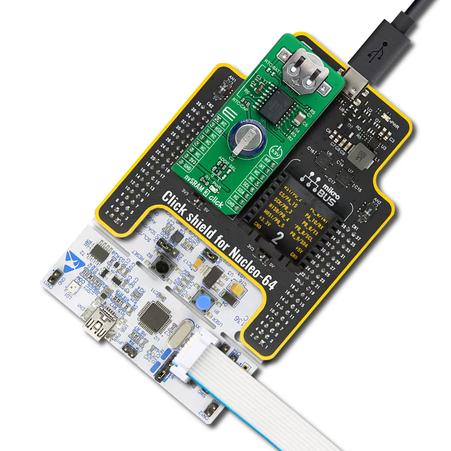
nvSRAM Click
Dev. board
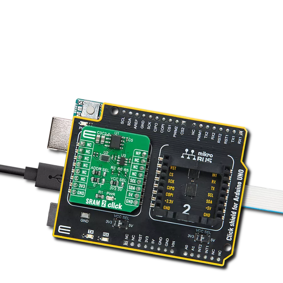
Arduino UNO Rev3
Compiler
NECTO Studio
MCU
ATmega328P
Our nvSRAM solution preserves your critical data, performs at lightning speed, and ensures data persistence without compromise
A
A
Hardware Overview
How does it work?
nvSRAM Click is based on the CY14B101J, a 1-Mbit nvSRAM organized as 128K words of 8 bits, each with a nonvolatile element in each memory cell from Infineon. The CY14B101J integrates SRAM and nonvolatile memory cells into a single nvSRAM cell. In the Normal mode, all reads and writes happen directly from and to the SRAM portion of the nvSRAM. This provides faster write and read access than nonvolatile memory technology such as EEPROM and Flash. The nvSRAM specifies one million endurance cycles for nonvolatile cells with data retention of a minimum of 20 years. In the event of system power loss, data from the SRAM is transferred to its nonvolatile cell using energy stored in a capacitor labeled as C2. During the Power-Up, data from the nonvolatile cell is
recalled automatically in the SRAM array and available to the user. During the Power-Down, the endurance cycle is consumed only when data transfer happens from the SRAM cells to nonvolatile cells. nvSRAM Click communicates with MCU using the standard I2C 2-Wire interface with a clock frequency of up to 100kHz in the Standard, up to 400kHz in the Fast, up to 1MHz in the FastPlus, and up to 3.4MHz in the High-Speed Mode. The CY14B101J offers zero cycle delay write operation with infinite SRAM write endurance. Besides, it also allows the choice of the least significant bit (LSB) of its I2C slave address by positioning SMD jumpers labeled as ADDR SEL to an appropriate position marked as 0 and 1. An additional feature of this Click board™ represents
the configurable Write Protection function labeled as WP routed on the PWM pin of the mikroBUS™ socket. The WP pin is an active-high pin that protects the entire memory and all registers from write operations. This pin must be held high to inhibit all the write operations. When this pin is high, all memory and register writes are prohibited, and the address counter is not incremented. This Click board™ can be operated only with a 3.3V logic voltage level. The board must perform appropriate logic voltage level conversion before using MCUs with different logic levels. Also, it comes equipped with a library containing functions and an example code that can be used as a reference for further development.

Features overview
Development board
Arduino UNO is a versatile microcontroller board built around the ATmega328P chip. It offers extensive connectivity options for various projects, featuring 14 digital input/output pins, six of which are PWM-capable, along with six analog inputs. Its core components include a 16MHz ceramic resonator, a USB connection, a power jack, an
ICSP header, and a reset button, providing everything necessary to power and program the board. The Uno is ready to go, whether connected to a computer via USB or powered by an AC-to-DC adapter or battery. As the first USB Arduino board, it serves as the benchmark for the Arduino platform, with "Uno" symbolizing its status as the
first in a series. This name choice, meaning "one" in Italian, commemorates the launch of Arduino Software (IDE) 1.0. Initially introduced alongside version 1.0 of the Arduino Software (IDE), the Uno has since become the foundational model for subsequent Arduino releases, embodying the platform's evolution.

Microcontroller Overview
MCU Card / MCU

Architecture
AVR
MCU Memory (KB)
32
Silicon Vendor
Microchip
Pin count
28
RAM (Bytes)
2048
You complete me!
Accessories
Click Shield for Arduino UNO has two proprietary mikroBUS™ sockets, allowing all the Click board™ devices to be interfaced with the Arduino UNO board without effort. The Arduino Uno, a microcontroller board based on the ATmega328P, provides an affordable and flexible way for users to try out new concepts and build prototypes with the ATmega328P microcontroller from various combinations of performance, power consumption, and features. The Arduino Uno has 14 digital input/output pins (of which six can be used as PWM outputs), six analog inputs, a 16 MHz ceramic resonator (CSTCE16M0V53-R0), a USB connection, a power jack, an ICSP header, and reset button. Most of the ATmega328P microcontroller pins are brought to the IO pins on the left and right edge of the board, which are then connected to two existing mikroBUS™ sockets. This Click Shield also has several switches that perform functions such as selecting the logic levels of analog signals on mikroBUS™ sockets and selecting logic voltage levels of the mikroBUS™ sockets themselves. Besides, the user is offered the possibility of using any Click board™ with the help of existing bidirectional level-shifting voltage translators, regardless of whether the Click board™ operates at a 3.3V or 5V logic voltage level. Once you connect the Arduino UNO board with our Click Shield for Arduino UNO, you can access hundreds of Click boards™, working with 3.3V or 5V logic voltage levels.

Used MCU Pins
mikroBUS™ mapper
Take a closer look
Click board™ Schematic

Step by step
Project assembly

Start by selecting your development board and Click board™. Begin with the Arduino UNO Rev3 as your development board.


Track your results in real time
Application Output
1. Application Output - In Debug mode, the 'Application Output' window enables real-time data monitoring, offering direct insight into execution results. Ensure proper data display by configuring the environment correctly using the provided tutorial.

2. UART Terminal - Use the UART Terminal to monitor data transmission via a USB to UART converter, allowing direct communication between the Click board™ and your development system. Configure the baud rate and other serial settings according to your project's requirements to ensure proper functionality. For step-by-step setup instructions, refer to the provided tutorial.

3. Plot Output - The Plot feature offers a powerful way to visualize real-time sensor data, enabling trend analysis, debugging, and comparison of multiple data points. To set it up correctly, follow the provided tutorial, which includes a step-by-step example of using the Plot feature to display Click board™ readings. To use the Plot feature in your code, use the function: plot(*insert_graph_name*, variable_name);. This is a general format, and it is up to the user to replace 'insert_graph_name' with the actual graph name and 'variable_name' with the parameter to be displayed.

Software Support
Library Description
This library contains API for nvSRAM Click driver.
Key functions:
nvsram_send_cmd- The function sends the desired command to the CY14B101J2nvsram_memory_write- The function writes a sequential data starting of the targeted 17-bit memory addressnvsram_memory_read- The function read a sequential data starting from the targeted 17-bit memory address
Open Source
Code example
The complete application code and a ready-to-use project are available through the NECTO Studio Package Manager for direct installation in the NECTO Studio. The application code can also be found on the MIKROE GitHub account.
/*!
 * @file main.c
 * @brief nvSRAM Click example
 *
 * # Description
 * This is an example that demonstrates the use of the nvSRAM Click board.
 * In this example, we write and then read data from nvSRAM memory.
 * Results are being sent to the Usart Terminal where you can track their changes.
 * All data logs write on USB uart changes approximately for every 5 sec.
 *
 * The demo application is composed of two sections :
 *
 * ## Application Init
 * Initialization driver enables - I2C, lock Serial Number write, disable Block Protection
 * and enable Memory Write, also write log.
 *
 * ## Application Task
 * Writing data to a memory address, then reading it back and logging it onto uart terminal.
 *
 * @author Stefan Ilic
 *
 */

#include "board.h"
#include "log.h"
#include "nvsram.h"

static nvsram_t nvsram;
static log_t logger;

char demo_data[ 9 ] = { 'm', 'i', 'k', 'r', 'o', 'E', 13 ,10 , 0 };
char read_data[ 9 ];
uint32_t mem_addr;

void application_init ( void ) {
    log_cfg_t log_cfg;  /**< Logger config object. */
    nvsram_cfg_t nvsram_cfg;  /**< Click config object. */

    /**
     * Logger initialization.
     * Default baud rate: 115200
     * Default log level: LOG_LEVEL_DEBUG
     * @note If USB_UART_RX and USB_UART_TX
     * are defined as HAL_PIN_NC, you will
     * need to define them manually for log to work.
     * See @b LOG_MAP_USB_UART macro definition for detailed explanation.
     */
    LOG_MAP_USB_UART( log_cfg );
    log_init( &logger, &log_cfg );
    log_info( &logger, " Application Init " );
    mem_addr = 1024;

    // Click initialization.
    nvsram_cfg_setup( &nvsram_cfg );
    NVSRAM_MAP_MIKROBUS( nvsram_cfg, MIKROBUS_1 );
    err_t init_flag = nvsram_init( &nvsram, &nvsram_cfg );
    if ( I2C_MASTER_ERROR == init_flag ) {
        log_error( &logger, " Application Init Error. " );
        log_info( &logger, " Please, run program again... " );

        for ( ; ; );
    }

    log_printf( &logger,  "  Serial Number Lock   \r\n" );
    log_printf( &logger, " None Block Protection \r\n" );
    nvsram_reg_write( &nvsram, NVSRAM_MEM_CTL_REG, NVSRAM_SNL | NVSRAM_BP_NONE );
    Delay_ms ( 100 );
    log_printf( &logger, " Enable Memory Write \r\n" );
    nvsram_enable_memory_write( &nvsram, NVSRAM_WRITE_MEMORY_ENABLE );
    Delay_ms ( 100 );

    log_info( &logger, " Application Task \r\n" );
}

void application_task ( void ) {
    log_printf( &logger, "  Write data : %s \r\n", demo_data );
    nvsram_memory_write( &nvsram, mem_addr, &demo_data[ 0 ], 9 );
    log_printf( &logger, "- - - - - - - - - - - - \r\n" );
    Delay_ms ( 100 );

    nvsram_memory_read( &nvsram, mem_addr, &read_data[ 0 ], 9 );
    log_printf( &logger, "  Read data  : %s \r\n", read_data );
    log_printf( &logger, "----------------------- \r\n" );
    Delay_ms ( 1000 );
    Delay_ms ( 1000 );
    Delay_ms ( 1000 );
    Delay_ms ( 1000 );
    Delay_ms ( 1000 );
}

int main ( void )
{
    /* Do not remove this line or clock might not be set correctly. */
    #ifdef PREINIT_SUPPORTED
    preinit();
    #endif

    application_init( );

    for ( ; ; )
    {
        application_task( );
    }

    return 0;
}

// ------------------------------------------------------------------------ END
Additional Support
Resources
Category:SRAM