Keep critical information readily available and secure with CY14B101PA and STM32G071RB
Data persistence perfected: The nvSRAM promise

Published Oct 08, 2024
Click board™
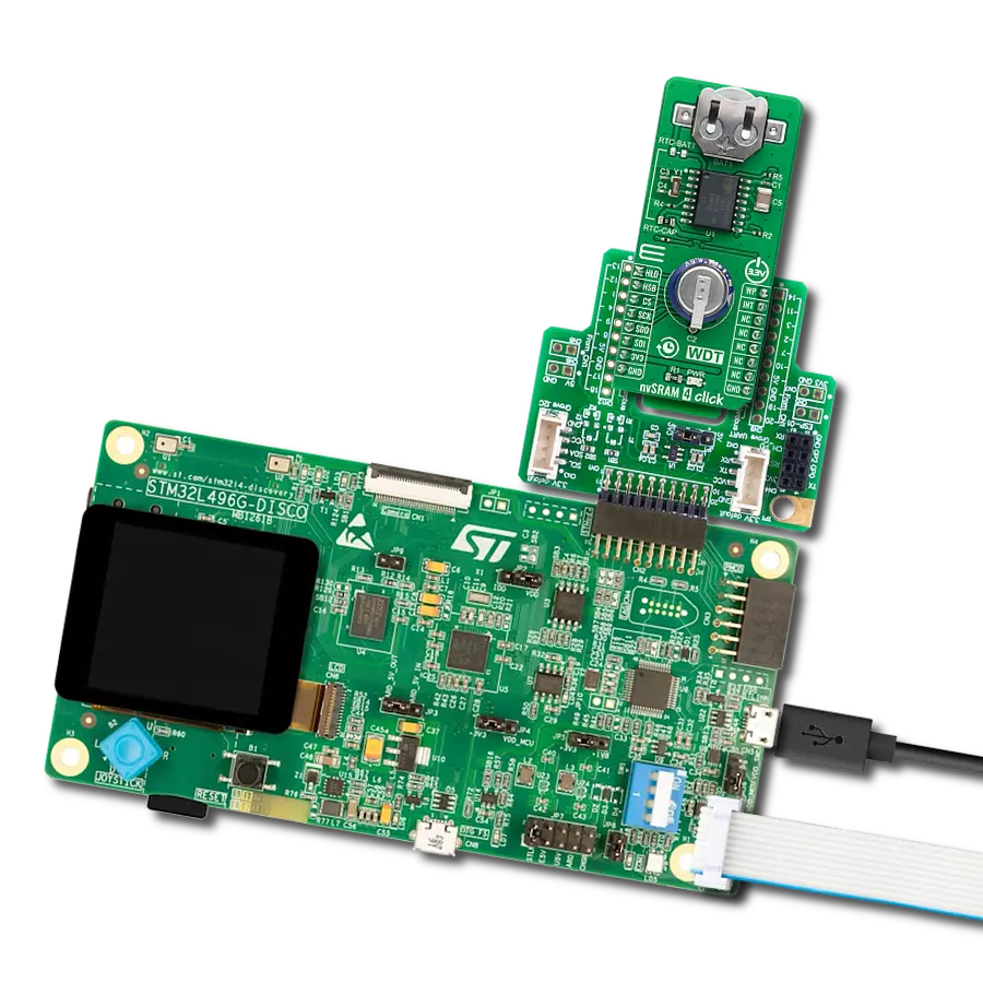
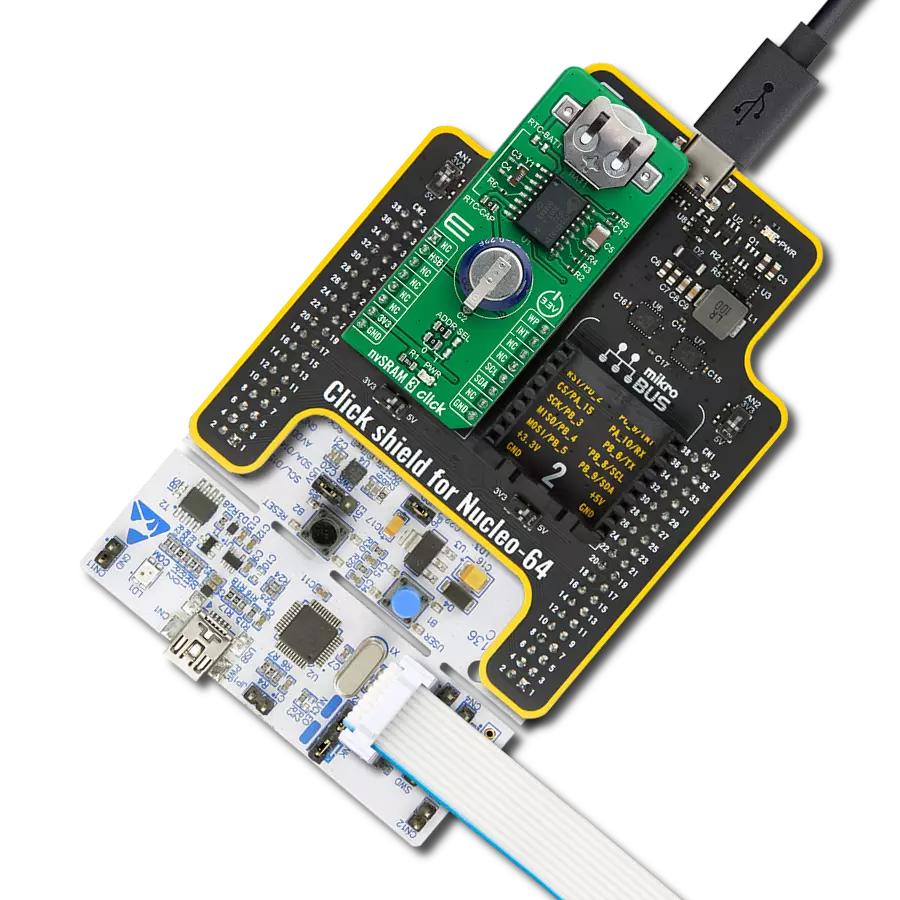
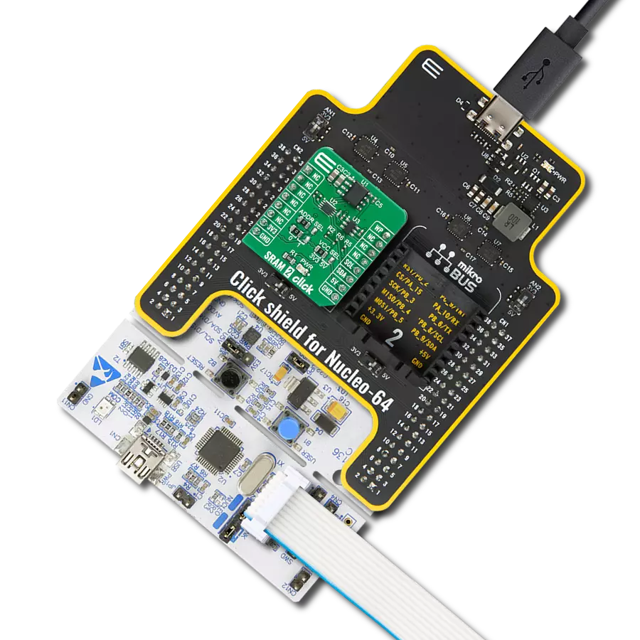
nvSRAM 4 Click
Dev. board
Nucleo 64 with STM32G071RB MCU
Compiler
NECTO Studio
MCU
STM32G071RB
Experience the perfect harmony of performance and peace of mind with nvSRAM, the ultimate memory solution for critical applications
A
A
Hardware Overview
How does it work?
nvSRAM 4 Click is based on the CY14B101PA, a 1-Mbit nvSRAM memory organized as 128K words of 8 bits each, with a fully-featured real-time clock from Infineon. The nvSRAM specifies one million endurance cycles for nonvolatile cells with data retention of a minimum of 20 years. All the reads and writes to nvSRAM happen to the SRAM, which gives nvSRAM the unique capability to handle infinite writes to the memory. The benefit of nvSRAM over serial EEPROMs is that all reads and writes to nvSRAM are performed at the SPI speed with zero cycle delay, which means, therefore, no wait time is required after any of the memory accesses. In addition to the CY14B101PA, this Click board™ is equipped with the button cell battery holder compatible with the 3000TR battery holder, suitable for 12mm Coin Cell batteries. When the primary power fails and drops below 2.65V, this Click board™ switches to the backup power supply by placing a jumper labeled as RTC-BATT. By utilizing an automatic backup, the CY14B101PA uses an external battery power source when there is no power supply on its main power terminals, allowing for uninterrupted operation. nvSRAM 4
Click communicates with MCU using a standard SPI interface with clock frequency up to 40MHz, zero cycle delay read, and write cycles. It also supports the two most common modes, SPI Mode 0 and 3, and 104 MHz SPI access speed with special instructions for the read operation. The CY14B101PA uses the standard SPI opcodes for memory access. In addition to the general SPI instructions for reading and writing, it provides four special instructions: STORE, RECALL, AutoStore Disable (ASDISB), and AutoStore Enable (ASENB). The STORE operation of the CY14B101PA can be controlled and acknowledged via the HSB pin, routed on the RST pin of the mikroBUS™ socket. If no STORE/RECALL is in progress, this pin can request a hardware STORE cycle. When the HSB pin is driven LOW, the CY14B101PA initiates a STORE operation conditionally. Also, this Click board™ can use the AutoStore feature of the SRAM data in nonvolatile cells when the power goes down, providing power-down data security by placing a jumper labeled as RTC-CAP. An additional feature of this Click board™ represents the configurable Write Protection function labeled
as WP routed on the PWM pin of the mikroBUS™ socket. The WP pin protects the entire memory and all registers from write operations and must be held high to inhibit all the write operations. When this pin is high, all memory and register writes are prohibited, and the address counter is not incremented. Besides, the nvSRAM 4 Click also has additional HOLD and Interrupt pins, routed to the AN and INT pins of the mikroBUS™ socket labeled as HLD and INT. The HLD pin is used to pause the serial communication without stopping the operation of the write status register, programming, or erasing in progress. On the other hand, an INT pin can be used in several ways, such as interrupt output, calibration, or a square wave, programmable to respond to the clock alarm, the watchdog timer, and the power monitor. This Click board™ can be operated only with a 3.3V logic voltage level. The board must perform appropriate logic voltage level conversion before using MCUs with different logic levels. Also, it comes equipped with a library containing functions and an example code that can be used as a reference for further development.

Features overview
Development board
Nucleo-64 with STM32G071RB MCU offers a cost-effective and adaptable platform for developers to explore new ideas and prototype their designs. This board harnesses the versatility of the STM32 microcontroller, enabling users to select the optimal balance of performance and power consumption for their projects. It accommodates the STM32 microcontroller in the LQFP64 package and includes essential components such as a user LED, which doubles as an ARDUINO® signal, alongside user and reset push-buttons, and a 32.768kHz crystal oscillator for precise timing operations. Designed with expansion and flexibility in mind, the Nucleo-64 board features an ARDUINO® Uno V3 expansion connector and ST morpho extension pin
headers, granting complete access to the STM32's I/Os for comprehensive project integration. Power supply options are adaptable, supporting ST-LINK USB VBUS or external power sources, ensuring adaptability in various development environments. The board also has an on-board ST-LINK debugger/programmer with USB re-enumeration capability, simplifying the programming and debugging process. Moreover, the board is designed to simplify advanced development with its external SMPS for efficient Vcore logic supply, support for USB Device full speed or USB SNK/UFP full speed, and built-in cryptographic features, enhancing both the power efficiency and security of projects. Additional connectivity is
provided through dedicated connectors for external SMPS experimentation, a USB connector for the ST-LINK, and a MIPI® debug connector, expanding the possibilities for hardware interfacing and experimentation. Developers will find extensive support through comprehensive free software libraries and examples, courtesy of the STM32Cube MCU Package. This, combined with compatibility with a wide array of Integrated Development Environments (IDEs), including IAR Embedded Workbench®, MDK-ARM, and STM32CubeIDE, ensures a smooth and efficient development experience, allowing users to fully leverage the capabilities of the Nucleo-64 board in their projects.

Microcontroller Overview
MCU Card / MCU
Architecture
ARM Cortex-M0
MCU Memory (KB)
128
Silicon Vendor
STMicroelectronics
Pin count
64
RAM (Bytes)
36864
You complete me!
Accessories
Click Shield for Nucleo-64 comes equipped with two proprietary mikroBUS™ sockets, allowing all the Click board™ devices to be interfaced with the STM32 Nucleo-64 board with no effort. This way, Mikroe allows its users to add any functionality from our ever-growing range of Click boards™, such as WiFi, GSM, GPS, Bluetooth, ZigBee, environmental sensors, LEDs, speech recognition, motor control, movement sensors, and many more. More than 1537 Click boards™, which can be stacked and integrated, are at your disposal. The STM32 Nucleo-64 boards are based on the microcontrollers in 64-pin packages, a 32-bit MCU with an ARM Cortex M4 processor operating at 84MHz, 512Kb Flash, and 96KB SRAM, divided into two regions where the top section represents the ST-Link/V2 debugger and programmer while the bottom section of the board is an actual development board. These boards are controlled and powered conveniently through a USB connection to program and efficiently debug the Nucleo-64 board out of the box, with an additional USB cable connected to the USB mini port on the board. Most of the STM32 microcontroller pins are brought to the IO pins on the left and right edge of the board, which are then connected to two existing mikroBUS™ sockets. This Click Shield also has several switches that perform functions such as selecting the logic levels of analog signals on mikroBUS™ sockets and selecting logic voltage levels of the mikroBUS™ sockets themselves. Besides, the user is offered the possibility of using any Click board™ with the help of existing bidirectional level-shifting voltage translators, regardless of whether the Click board™ operates at a 3.3V or 5V logic voltage level. Once you connect the STM32 Nucleo-64 board with our Click Shield for Nucleo-64, you can access hundreds of Click boards™, working with 3.3V or 5V logic voltage levels.

Used MCU Pins
mikroBUS™ mapper
Take a closer look
Click board™ Schematic

Step by step
Project assembly
Start by selecting your development board and Click board™. Begin with the Nucleo 64 with STM32G071RB MCU as your development board.


Software Support
Library Description
This library contains API for nvSRAM 4 Click driver.
Key functions:
nvsram4_burst_read_memory- nvSRAM 4 burst read memory function.nvsram4_burst_write_memory- nvSRAM 4 burst write memory function.nvsram4_get_rtc_time- nvSRAM 4 get RTC time function.
Open Source
Code example
The complete application code and a ready-to-use project are available through the NECTO Studio Package Manager for direct installation in the NECTO Studio. The application code can also be found on the MIKROE GitHub account.
/*!
 * @file main.c
 * @brief nvSRAM4 Click example
 *
 * # Description
 * This is an example that demonstrates the use of the nvSRAM 4 Click board.
 *
 * The demo application is composed of two sections :
 *
 * ## Application Init
 * Initialization driver enables - SPI,
 * write demo_data string ( mikroE ), starting from the selected memory_addr ( 112233 ),
 * set the time to 12:30:31 and set the date to 31-12-20.
 *
 * ## Application Task
 * In this example, we read a data string, which we have previously written to memory,
 * starting from the selected memory_addr ( 112233 )
 * and read and display the current time and date, which we also previously set.
 * Results are being sent to the Usart Terminal where you can track their changes.
 * All data logs write on USB uart changes for every 1 sec.
 *
 * @author Nenad Filipovic
 *
 */

#include "board.h"
#include "log.h"
#include "nvsram4.h"

static nvsram4_t nvsram4;
static log_t logger;

static char demo_data[ 9 ] = { 'm', 'i', 'k', 'r', 'o', 'E', 13 ,10 , 0 };
static char rx_data[ 9 ];
static uint32_t memory_addr;
static uint8_t new_sec = 255;
static uint8_t c_year = 20;

static nvsram4_rtc_time_t time;
static nvsram4_rtc_date_t date;

void application_init ( void ) {
    log_cfg_t log_cfg;          /**< Logger config object. */
    nvsram4_cfg_t nvsram4_cfg;  /**< Click config object. */

    /**
     * Logger initialization.
     * Default baud rate: 115200
     * Default log level: LOG_LEVEL_DEBUG
     * @note If USB_UART_RX and USB_UART_TX
     * are defined as HAL_PIN_NC, you will
     * need to define them manually for log to work.
     * See @b LOG_MAP_USB_UART macro definition for detailed explanation.
     */
    LOG_MAP_USB_UART( log_cfg );
    log_init( &logger, &log_cfg );
    log_printf( &logger, "\r\n" );
    log_info( &logger, " Application Init " );

    // Click initialization.

    nvsram4_cfg_setup( &nvsram4_cfg );
    NVSRAM4_MAP_MIKROBUS( nvsram4_cfg, MIKROBUS_1 );
    err_t init_flag  = nvsram4_init( &nvsram4, &nvsram4_cfg );
    if ( init_flag == SPI_MASTER_ERROR ) {
        log_error( &logger, " Application Init Error. " );
        log_info( &logger, " Please, run program again... " );

        for ( ; ; );
    }

    nvsram4_default_cfg ( &nvsram4 );
    Delay_ms ( 100 );
    log_info( &logger, " Application Task " );

    log_printf( &logger, "-----------------------\r\n" );
    log_printf( &logger, "     nvSRAM 4 Click    \r\n" );
    log_printf( &logger, "-----------------------\r\n" );

    memory_addr = 112233;

    nvsram4_set_cmd( &nvsram4, NVSRAM4_STATUS_WREN );
    Delay_ms ( 100 );

    log_printf( &logger, "  Write data : %s", demo_data );
    nvsram4_burst_write_memory( &nvsram4, memory_addr, &demo_data[ 0 ], 9 );
    log_printf( &logger, "-----------------------\r\n" );
    Delay_ms ( 1000 );

    date.day_of_week = 4;
    date.day = 31;
    date.month = 12;
    date.year = 20;
    nvsram4_set_rtc_date( &nvsram4, date );
    Delay_ms ( 100 );

    time.hours = 23;
    time.min = 59;
    time.sec = 50;
    nvsram4_set_rtc_time( &nvsram4, time );
    Delay_ms ( 100 );
}

void application_task ( void ) {
    nvsram4_get_rtc_time( &nvsram4, &time );
    Delay_ms ( 1 );
    nvsram4_get_rtc_date( &nvsram4, &date );
    Delay_ms ( 1 );

    if ( time.sec != new_sec ) {
        log_printf( &logger, "  Date      : %.2d-%.2d-%.2d\r\n", ( uint16_t ) date.day, ( uint16_t ) date.month, ( uint16_t ) date.year );
        log_printf( &logger, "  Time      : %.2d:%.2d:%.2d\r\n", ( uint16_t ) time.hours, ( uint16_t ) time.min, ( uint16_t ) time.sec );
        log_printf( &logger, "- - - - - - - - - - - -\r\n" );
        new_sec = time.sec;
        Delay_ms ( 10 );

        if ( date.year != c_year ) {
            log_printf( &logger, "     Happy New Year    \r\n" );
            c_year = date.year;
            Delay_ms ( 10 );
        } else {
            nvsram4_burst_read_memory( &nvsram4, memory_addr, &rx_data[ 0 ], 9 );
            log_printf( &logger, "  Read data : %s", rx_data );
        }

        log_printf( &logger, "-----------------------\r\n" );
    } else {
        Delay_ms ( 1 );
    }
}

int main ( void )
{
    /* Do not remove this line or clock might not be set correctly. */
    #ifdef PREINIT_SUPPORTED
    preinit();
    #endif

    application_init( );

    for ( ; ; )
    {
        application_task( );
    }

    return 0;
}

// ------------------------------------------------------------------------ END
Additional Support
Resources
Category:SRAM