Process data swiftly thanks to the ANV32AA1WDK66 and STM32F413ZH, no matter the task
Unlock unprecedented speed with our SRAM solution
Published Feb 14, 2024
Click board™
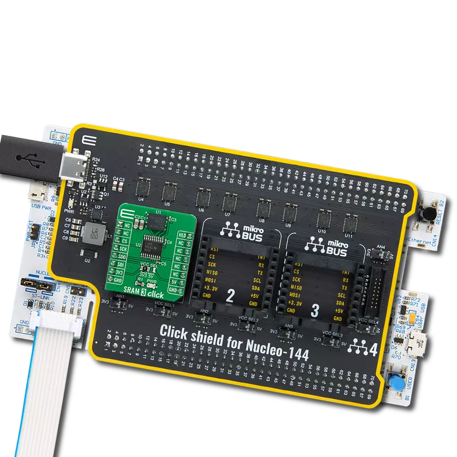
SRAM 3 Click
Dev. board
Nucleo 144 with STM32F413ZH MCU
Compiler
NECTO Studio
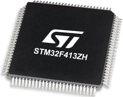
MCU
STM32F413ZH
With our SRAM memory, you can trust in data integrity and fast access for critical operations
A
A
Hardware Overview
How does it work?
SRAM 3 Click is based on the ANV32AA1WDK66, a serial non-volatile SRAM with double memory architecture and SPI serial interface organized as 128k words of 8 bits each from Anvo-System Dresden. This memory has a silicon-oxide-nitride-oxide-silicon (SONOS) flash storage element included with each memory cell. In the case of an unforeseeable operating voltage drop below a defined value, the SONOS technology enables non-volatile data storage in less than 15ms. An integrated Power Down functionality of the SRAM 3 Click with a standby current of less than 1µA ensures low power consumption, with recovery time from Power-Down Mode typically of 60µs. This ANV32AA1WDK66 possesses unique safety features, such as Checksum Protected Memory Accesses (Secure READ and Secure WRITE instructions) and Time Monitoring that ensures a
high degree of reliability of this Click board™. Corrupt data cannot overwrite existing memory content; even valid data would not overwrite on a corrupted address. The SRAM 3 Click also provides some distinctive advantages of SRAMs, such as fast access times and unlimited write/read endurance. SRAM 3 Click incorporates an additional IC, the TXB0108PWR, an 8-bit bidirectional voltage level translator from Texas Instruments. This allows the Click board™ to be used with a much more extensive range of MCUs. At the same time, the TXB0108PWR protects the ANV32AA1WDK66 from the Electrostatic Discharges (ESD) up to ±15 kV, making SRAM 3 Click a very reliable embedded storage solution. The ANV32AA1WDK66 communicates with MCU using the standard SPI serial interface that supports modes 0 and 3 with a maximum
frequency of 66 MHz. It also possesses an additional HOLD function routed at the PWM pin of the mikroBUS™ socket labeled as HLD. This pin is used with the CS pin to select the device. When the device is selected, and a serial sequence is underway, an HLD pin can pause the serial communication with the host device without resetting the serial sequence. This Click board™ can operate with either 3.3V or 5V logic voltage levels selected via the VCC SEL jumper. This way, both 3.3V and 5V capable MCUs can use the communication lines properly. Also, this Click board™ comes equipped with a library containing easy-to-use functions and an example code that can be used as a reference for further development.

Features overview
Development board
Nucleo-144 with STM32F413ZH MCU board offers an accessible and adaptable avenue for users to explore new ideas and construct prototypes. It allows users to tailor their experience by selecting from a range of performance and power consumption features offered by the STM32 microcontroller. With compatible boards, the
internal or external SMPS dramatically decreases power usage in Run mode. Including the ST Zio connector, expanding ARDUINO Uno V3 connectivity, and ST morpho headers facilitate easy expansion of the Nucleo open development platform. The integrated ST-LINK debugger/programmer enhances convenience by
eliminating the need for a separate probe. Moreover, the board is accompanied by comprehensive free software libraries and examples within the STM32Cube MCU Package, further enhancing its utility and value.

Microcontroller Overview
MCU Card / MCU
Architecture
ARM Cortex-M4
MCU Memory (KB)
1536
Silicon Vendor
STMicroelectronics
Pin count
144
RAM (Bytes)
327680
You complete me!
Accessories
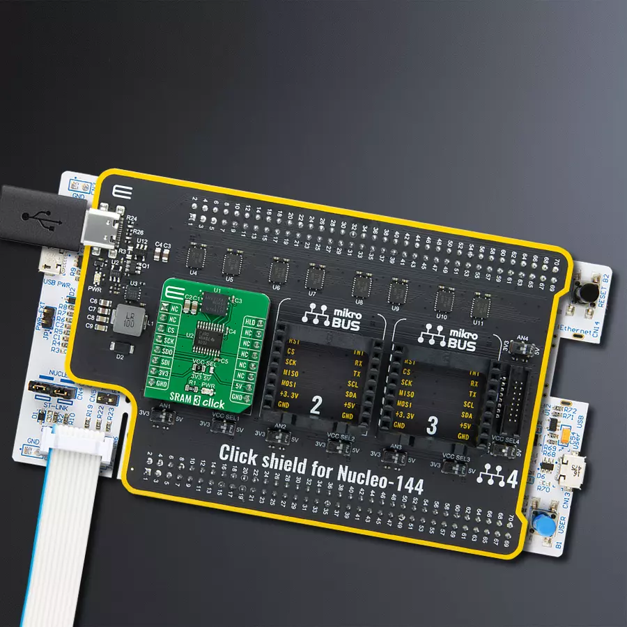
Click Shield for Nucleo-144 comes equipped with four mikroBUS™ sockets, with one in the form of a Shuttle connector, allowing all the Click board™ devices to be interfaced with the STM32 Nucleo-144 board with no effort. This way, MIKROE allows its users to add any functionality from our ever-growing range of Click boards™, such as WiFi, GSM, GPS, Bluetooth, ZigBee, environmental sensors, LEDs, speech recognition, motor control, movement sensors, and many more. Featuring an ARM Cortex-M microcontroller, 144 pins, and Arduino™ compatibility, the STM32 Nucleo-144 board offers limitless possibilities for prototyping and creating diverse applications. These boards are controlled and powered conveniently through a USB connection to program and efficiently debug the Nucleo-144 board out of the box, with an additional USB cable connected to the USB mini port on the board. Simplify your project development with the integrated ST-Link debugger and unleash creativity using the extensive I/O options and expansion capabilities. This Click Shield also has several switches that perform functions such as selecting the logic levels of analog signals on mikroBUS™ sockets and selecting logic voltage levels of the mikroBUS™ sockets themselves. Besides, the user is offered the possibility of using any Click board™ with the help of existing bidirectional level-shifting voltage translators, regardless of whether the Click board™ operates at a 3.3V or 5V logic voltage level. Once you connect the STM32 Nucleo-144 board with our Click Shield for Nucleo-144, you can access hundreds of Click boards™, working with 3.3V or 5V logic voltage levels.

Used MCU Pins
mikroBUS™ mapper
Take a closer look
Click board™ Schematic

Step by step
Project assembly
Start by selecting your development board and Click board™. Begin with the Nucleo 144 with STM32F413ZH MCU as your development board.


Track your results in real time
Application Output
1. Application Output - In Debug mode, the 'Application Output' window enables real-time data monitoring, offering direct insight into execution results. Ensure proper data display by configuring the environment correctly using the provided tutorial.

2. UART Terminal - Use the UART Terminal to monitor data transmission via a USB to UART converter, allowing direct communication between the Click board™ and your development system. Configure the baud rate and other serial settings according to your project's requirements to ensure proper functionality. For step-by-step setup instructions, refer to the provided tutorial.

3. Plot Output - The Plot feature offers a powerful way to visualize real-time sensor data, enabling trend analysis, debugging, and comparison of multiple data points. To set it up correctly, follow the provided tutorial, which includes a step-by-step example of using the Plot feature to display Click board™ readings. To use the Plot feature in your code, use the function: plot(*insert_graph_name*, variable_name);. This is a general format, and it is up to the user to replace 'insert_graph_name' with the actual graph name and 'variable_name' with the parameter to be displayed.

Software Support
Library Description
This library contains API for SRAM 3 Click driver.
Key functions:
sram3_enable_write- This function is for enabling writing to memory, status register or user serial.sram3_disable_write- Function for disabling writing to memory, status register or user serial.sram3_protect_memory- Function which secures part of memory from writing.
Open Source
Code example
The complete application code and a ready-to-use project are available through the NECTO Studio Package Manager for direct installation in the NECTO Studio. The application code can also be found on the MIKROE GitHub account.
/*!
 * @file main.c
 * @brief SRAM3 Click example
 *
 * # Description
 * This is an example that shows the use of SRAM memory, using SRAM 3 Click. SRAM 3 Click is based on ANV32AA1W,
 * and ANV32AA1W is a 1Mb serial SRAM with a non-volatile SONOS storage element included with each memory cell,
 * organized as 128k words of 8 bits each. The devices are accessed by a high speed SPI-compatible bus.
 * Specifically in this example, we used the high-speed SPI communication characteristics to write data to a specific
 * registration address and read it.
 *
 * The demo application is composed of two sections :
 *
 * ## Application Init
 * Initialization SPI module, logger initalization and Click initialization.
 *
 * ## Application Task
 * First, we write the data to the registry address 0x00, and then we read the data from 0x00 address.
 *
 * @author Jelena Milosavljevic
 *
 */

#include "board.h"
#include "log.h"
#include "sram3.h"

static sram3_t sram3;
static log_t logger;
uint8_t buf[10] = { 'M','i','k','r','o','E', 0 };

void application_init ( void ) {
    log_cfg_t log_cfg;         /**< Logger config object. */
    sram3_cfg_t sram3_cfg;     /**< Click config object. */

    /**
     * Logger initialization.
     * Default baud rate: 115200
     * Default log level: LOG_LEVEL_DEBUG
     * @note If USB_UART_RX and USB_UART_TX
     * are defined as HAL_PIN_NC, you will
     * need to define them manually for log to work.
     * See @b LOG_MAP_USB_UART macro definition for detailed explanation.
     */
    LOG_MAP_USB_UART( log_cfg );
    log_init( &logger, &log_cfg );
    log_info( &logger, " Application Init " );

    // Click initialization.
    sram3_cfg_setup( &sram3_cfg );
    SRAM3_MAP_MIKROBUS( sram3_cfg, MIKROBUS_1 );
    err_t init_flag  = sram3_init( &sram3, &sram3_cfg );
    if ( SPI_MASTER_ERROR == init_flag ) {
        log_error( &logger, " Application Init Error. " );
        log_info( &logger, " Please, run program again... " );
        for ( ; ; );
    }

    log_info( &logger, " Application Task " );
    sram3_release_hold( &sram3 );
    Delay_ms ( 100 );
}

void application_task ( void ) {
    char buff_out[ 10 ] = { 0 };

    log_printf( &logger, "Writing [ %s ] to memory...\r\n", buf );
    sram3_enable_write( &sram3 );
    sram3_write( &sram3, 0x00, &buf[0], 6 );

    Delay_ms ( 100 );
    sram3_read( &sram3, 0x00, &buff_out[0], 6 );
    Delay_ms ( 100 );
    log_printf( &logger, "Data read from memory: %s \r\n", buff_out );
    log_printf( &logger, "---------------------------------------------\r\n" );

    Delay_ms ( 1000 );
    Delay_ms ( 1000 );
}

int main ( void )
{
    /* Do not remove this line or clock might not be set correctly. */
    #ifdef PREINIT_SUPPORTED
    preinit();
    #endif

    application_init( );

    for ( ; ; )
    {
        application_task( );
    }

    return 0;
}

// ------------------------------------------------------------------------ END
Additional Support
Resources
Category:SRAM