Encode analog signal into a binary code easily with ADS7828 and STM32F091RC
Convert with clarity

Published Feb 26, 2024
Click board™
ADC 12 Click
Dev. board
Nucleo-64 with STM32F091RC MCU
Compiler
NECTO Studio
MCU
STM32F091RC
Ready to take on even the most complex designs? Our ADC is up to the challenge!
A
A
Hardware Overview
How does it work?
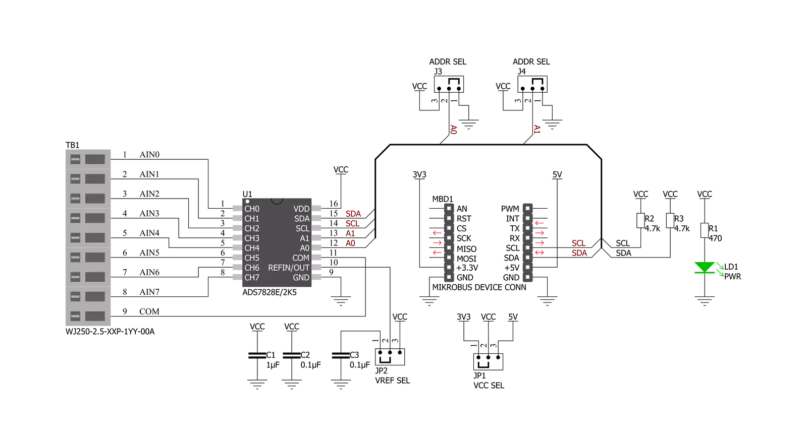
ADC 12 Click is based on the ADS7828, a low-power 12-bit data acquisition device with a serial I2C interface and an 8-channel multiplexer from Texas Instruments. The architecture of the ADS7828, which is a classic Successive Approximation Register (SAR) A/D converter, is based on capacitive redistribution that inherently includes a sample-and-hold function. It has an integrated I2C input and output port with screw terminal connectors for each analog input channel. An internally generated free-running clock controls it. When the ADS7828 is not performing conversions or being addressed, it keeps the A/D converter core powered off, and the internal clock does not operate. When the A/D converter enters the Hold mode, the voltage on the selected channel pin of the input
terminal is captured on the internal capacitor array. The input current on the analog inputs depends on the conversion rate of the device. During the sample period, the source must charge the internal sampling capacitor. There is no further input current after the capacitor has been fully charged. The amount of charge transfer from the analog source to the converter is a function of the conversion rate. ADC 12 Click communicates with MCU using the standard I2C 2-Wire interface with a frequency of up to 100kHz in the Standard, up to 400kHz in the Fast, and up to 3.4MHz in the High-Speed mode. It also allows the choice of the last two least significant bits (LSB), A0 and A1, by positioning SMD jumpers labeled ADDR SEL to an appropriate position marked as 0 and 1.
This Click board™ also possesses a jumper for selecting the reference voltage labeled as VREF SEL. The ADS7828 can operate with an internal 2.5V reference or an external reference (in this case, logic voltage level VCC), which can be selected by positioning SMD jumpers to an appropriate position marked as INT and EXT. This Click board™ can operate with either 3.3V or 5V logic voltage levels selected via the VCC SEL jumper. This way, both 3.3V and 5V capable MCUs can use the communication lines properly. However, the Click board™ comes equipped with a library containing easy-to-use functions and an example code that can be used, as a reference, for further development.


Features overview
Development board
Nucleo-64 with STM32F091RC MCU offers a cost-effective and adaptable platform for developers to explore new ideas and prototype their designs. This board harnesses the versatility of the STM32 microcontroller, enabling users to select the optimal balance of performance and power consumption for their projects. It accommodates the STM32 microcontroller in the LQFP64 package and includes essential components such as a user LED, which doubles as an ARDUINO® signal, alongside user and reset push-buttons, and a 32.768kHz crystal oscillator for precise timing operations. Designed with expansion and flexibility in mind, the Nucleo-64 board features an ARDUINO® Uno V3 expansion connector and ST morpho extension pin
headers, granting complete access to the STM32's I/Os for comprehensive project integration. Power supply options are adaptable, supporting ST-LINK USB VBUS or external power sources, ensuring adaptability in various development environments. The board also has an on-board ST-LINK debugger/programmer with USB re-enumeration capability, simplifying the programming and debugging process. Moreover, the board is designed to simplify advanced development with its external SMPS for efficient Vcore logic supply, support for USB Device full speed or USB SNK/UFP full speed, and built-in cryptographic features, enhancing both the power efficiency and security of projects. Additional connectivity is
provided through dedicated connectors for external SMPS experimentation, a USB connector for the ST-LINK, and a MIPI® debug connector, expanding the possibilities for hardware interfacing and experimentation. Developers will find extensive support through comprehensive free software libraries and examples, courtesy of the STM32Cube MCU Package. This, combined with compatibility with a wide array of Integrated Development Environments (IDEs), including IAR Embedded Workbench®, MDK-ARM, and STM32CubeIDE, ensures a smooth and efficient development experience, allowing users to fully leverage the capabilities of the Nucleo-64 board in their projects.

Microcontroller Overview
MCU Card / MCU

Architecture
ARM Cortex-M0
MCU Memory (KB)
256
Silicon Vendor
STMicroelectronics
Pin count
64
RAM (Bytes)
32768
You complete me!
Accessories
Click Shield for Nucleo-64 comes equipped with two proprietary mikroBUS™ sockets, allowing all the Click board™ devices to be interfaced with the STM32 Nucleo-64 board with no effort. This way, Mikroe allows its users to add any functionality from our ever-growing range of Click boards™, such as WiFi, GSM, GPS, Bluetooth, ZigBee, environmental sensors, LEDs, speech recognition, motor control, movement sensors, and many more. More than 1537 Click boards™, which can be stacked and integrated, are at your disposal. The STM32 Nucleo-64 boards are based on the microcontrollers in 64-pin packages, a 32-bit MCU with an ARM Cortex M4 processor operating at 84MHz, 512Kb Flash, and 96KB SRAM, divided into two regions where the top section represents the ST-Link/V2 debugger and programmer while the bottom section of the board is an actual development board. These boards are controlled and powered conveniently through a USB connection to program and efficiently debug the Nucleo-64 board out of the box, with an additional USB cable connected to the USB mini port on the board. Most of the STM32 microcontroller pins are brought to the IO pins on the left and right edge of the board, which are then connected to two existing mikroBUS™ sockets. This Click Shield also has several switches that perform functions such as selecting the logic levels of analog signals on mikroBUS™ sockets and selecting logic voltage levels of the mikroBUS™ sockets themselves. Besides, the user is offered the possibility of using any Click board™ with the help of existing bidirectional level-shifting voltage translators, regardless of whether the Click board™ operates at a 3.3V or 5V logic voltage level. Once you connect the STM32 Nucleo-64 board with our Click Shield for Nucleo-64, you can access hundreds of Click boards™, working with 3.3V or 5V logic voltage levels.

Used MCU Pins
mikroBUS™ mapper
Take a closer look
Click board™ Schematic
Step by step
Project assembly
Start by selecting your development board and Click board™. Begin with the Nucleo-64 with STM32F091RC MCU as your development board.


Software Support
Library Description
This library contains API for ADC 12 Click driver.
Key functions:
void adc12_send_cmd ( uint8_t cmd_byte );- Function is used to configure the device.uint16_t adc12_single_ended ( uint8_t chan, uint16_t v_ref );- Function is used to get raw ADC value.uint16_t adc12_differential ( uint8_t chan, uint16_t v_ref );- Function is used to get raw ADC value.
Open Source
Code example
The complete application code and a ready-to-use project are available through the NECTO Studio Package Manager for direct installation in the NECTO Studio. The application code can also be found on the MIKROE GitHub account.
/*!
 * @file main.c
 * @brief ADC12 Click example
 *
 * # Description
 * This example demonstrates the use of ADC 12 Click board.
 *
 * The demo application is composed of two sections :
 *
 * ## Application Init
 * Initializes the driver and sets the input and power-down modes.
 *
 * ## Application Task
 * Reads the RAW ADC data and converts it to voltage in milivolts and displays
 * both values on the USB UART every second.
 *
 * @note
 * With internal reference voltage set the Click measures up to 2500 mV.
 *
 * @author Stefan Filipovic
 *
 */

#include "board.h"
#include "log.h"
#include "adc12.h"

static adc12_t adc12;
static log_t logger;

void application_init ( void )
{
    log_cfg_t log_cfg;  /**< Logger config object. */
    adc12_cfg_t adc12_cfg;  /**< Click config object. */

    /**
     * Logger initialization.
     * Default baud rate: 115200
     * Default log level: LOG_LEVEL_DEBUG
     * @note If USB_UART_RX and USB_UART_TX
     * are defined as HAL_PIN_NC, you will
     * need to define them manually for log to work.
     * See @b LOG_MAP_USB_UART macro definition for detailed explanation.
     */
    LOG_MAP_USB_UART( log_cfg );
    log_init( &logger, &log_cfg );
    log_info( &logger, " Application Init " );

    // Click initialization.

    adc12_cfg_setup( &adc12_cfg );
    ADC12_MAP_MIKROBUS( adc12_cfg, MIKROBUS_1 );
    err_t init_flag = adc12_init( &adc12, &adc12_cfg );
    if ( init_flag == I2C_MASTER_ERROR )
    {
        log_error( &logger, " Application Init Error. " );
        log_info( &logger, " Please, run program again... " );

        for ( ; ; );
    }

    adc12_set_sd_mode ( &adc12, ADC12_CMD_SD_SINGLE_END );
    adc12_set_pd_mode( &adc12, ADC12_CMD_PD_IRON_ADON );
    log_info( &logger, " Application Task " );
}

void application_task ( void )
{
    uint16_t raw_adc;
    float voltage;

    adc12_read_raw_data ( &adc12, ADC12_SINGLE_END_CH0, &raw_adc );
    adc12_read_voltage ( &adc12, ADC12_SINGLE_END_CH0, ADC12_INTERNAL_VREF, &voltage );

    log_printf( &logger, " RAW ADC: %u \r\n", raw_adc );
    log_printf( &logger, " Voltage from Channel 0: %.2f mV \r\n", voltage );
    log_printf( &logger, " ---------------------------\r\n" );
    Delay_ms ( 1000 );
}

int main ( void )
{
    /* Do not remove this line or clock might not be set correctly. */
    #ifdef PREINIT_SUPPORTED
    preinit();
    #endif

    application_init( );

    for ( ; ; )
    {
        application_task( );
    }

    return 0;
}

// ------------------------------------------------------------------------ END
Additional Support
Resources
Category:ADC


