Ensure seamless journeys and hassle-free adventures with ORG1411 and STM32G071RB
Navigate with ease, every time

Published Oct 08, 2024
Click board™
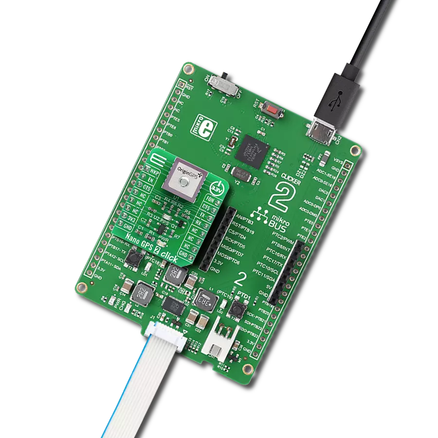
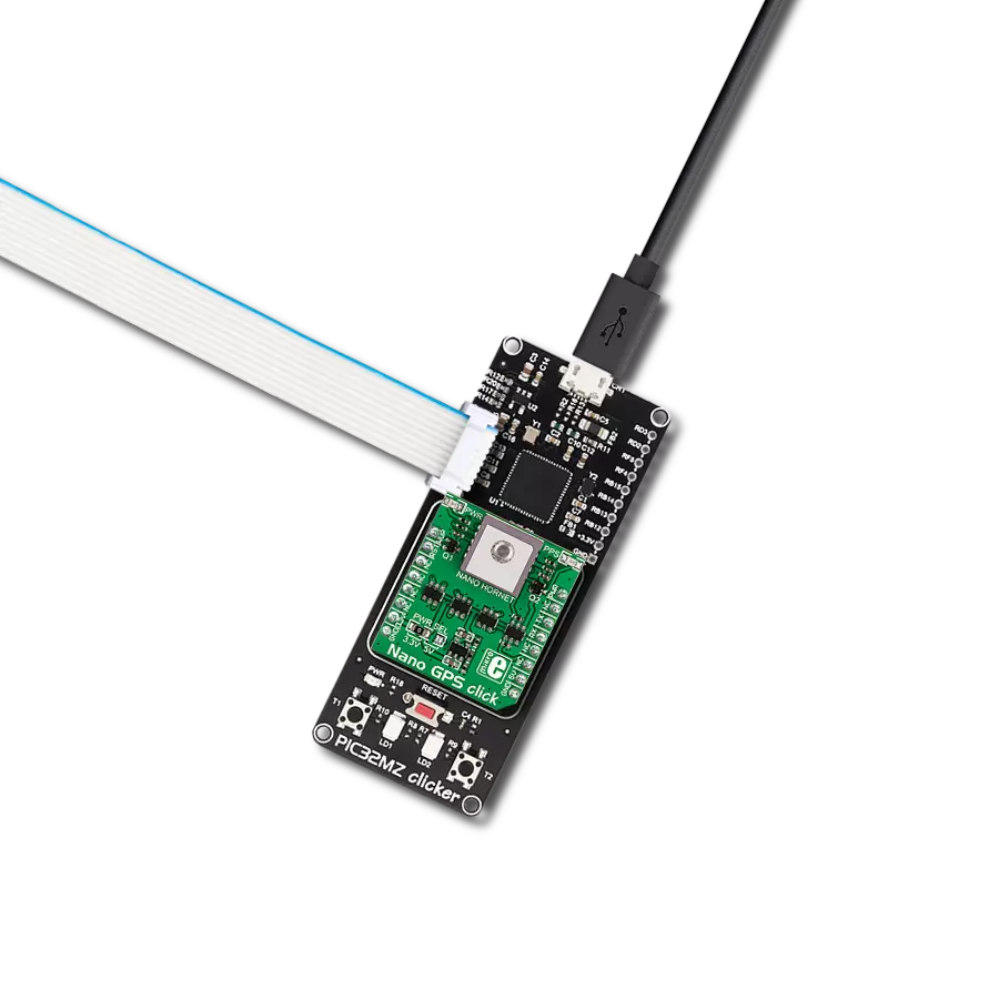
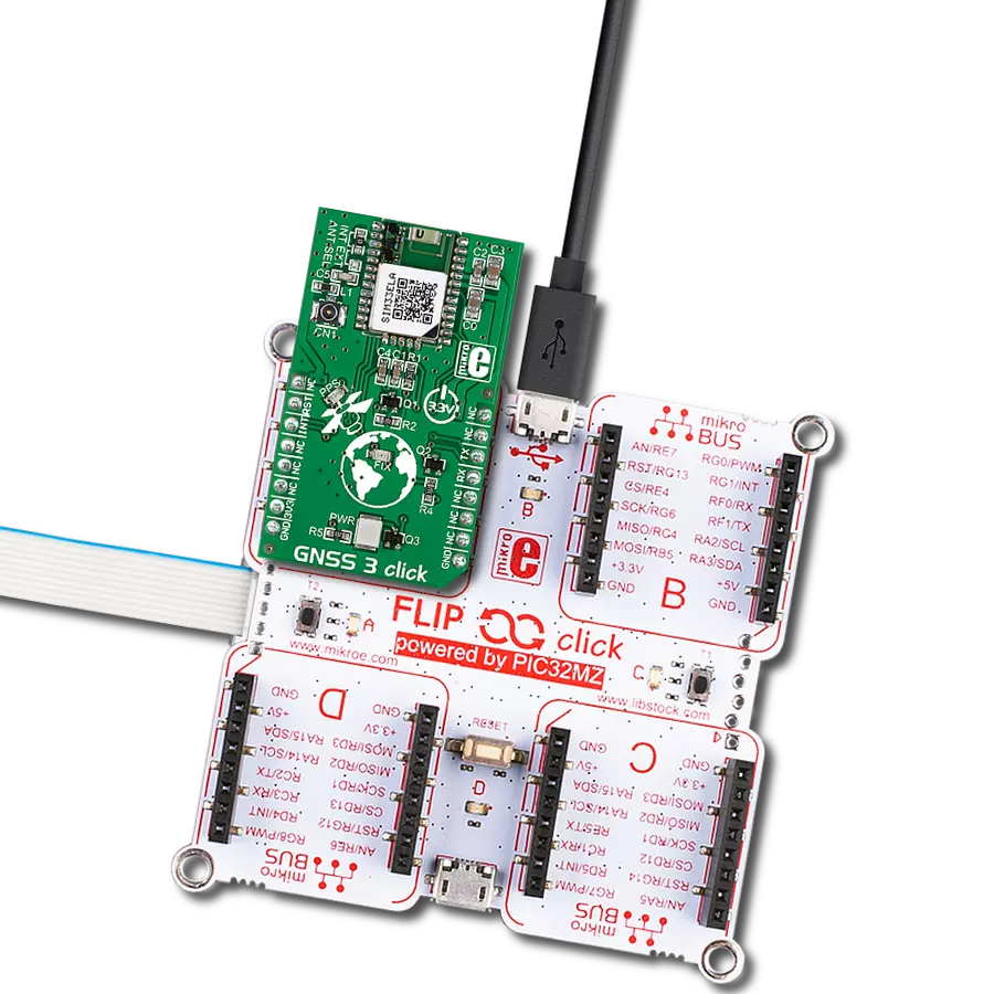
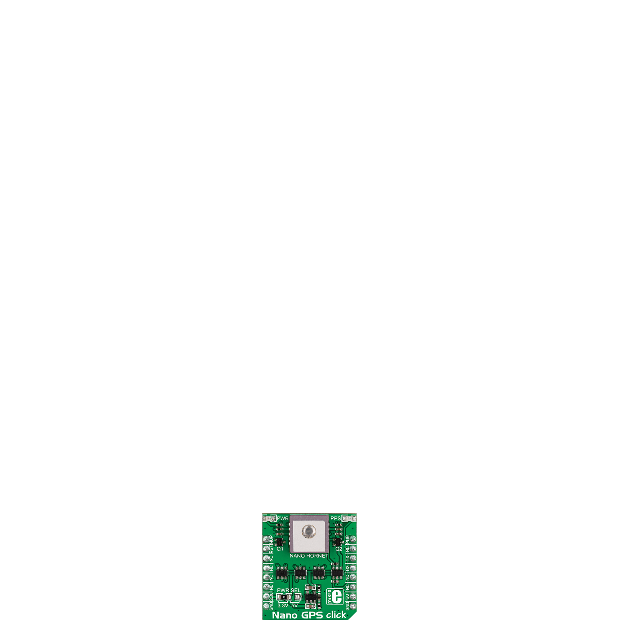
NANO GPS Click
Dev. board
Nucleo 64 with STM32G071RB MCU
Compiler
NECTO Studio
MCU
STM32G071RB
Individuals and adventurers benefit from our GPS solution by gaining accurate location information, enabling them to explore confidently and discover new horizons
A
A
Hardware Overview
How does it work?
Nano GPS Click is based on the Nano Hornet ORG1411, a complete SiP GPS Patch-on-Top (PoT) module from OriginGPS. The GPS module supports the L1 band only at 1575.42MHz for GPS, with 48 channels. The module is an ultra-low tracking power consumption device with a high sensitivity of -163dBm while tracking and -162dBm in reacquisition mode with less than 1 second of reacquisition time. The larger number of visible satellites increases horizontal positioning accuracy (<2.5m CEP) and decreases acquisition time (<1s TTFF with a hot start and <32 with a warm start). Nano GPS Click supports an active jammer detector/remover and better positioning under
signal conditions with onboard dual-stage LNA for better sensitivity. It also features OriginGPS Noise Free Zone System (NFZ™) technology, Autonomous and Predictive A-GPS, Ephemeris Push, Almanac-based Positioning, and more. As the module works on 1.8V, this Click board™ uses four voltage translators, the 74LVC1T45 from Diodes Incorporated, for all data lines connected with the host MCU, except for the RST signal for resetting the device. The ORG1411 uses the UART interface with commonly used UART RX and TX pins as its default communication protocol to transmit and exchange data for communication with the host MCU. The Power State Control pin
PWR switches the module between different power states, such as Hibernate, STP, PTF, and Full Power. The WUP pin is output from the module and indicates its power state, while the PPS LED provides a visual pulse signal for timing purposes. This Click board™ can operate with either 3.3V or 5V logic voltage levels selected via the PWR SEL jumper. This way, both 3.3V and 5V capable MCUs can use the communication lines properly. Also, this Click board™ comes equipped with a library containing easy-to-use functions and an example code that can be used as a reference for further development.

Features overview
Development board
Nucleo-64 with STM32G071RB MCU offers a cost-effective and adaptable platform for developers to explore new ideas and prototype their designs. This board harnesses the versatility of the STM32 microcontroller, enabling users to select the optimal balance of performance and power consumption for their projects. It accommodates the STM32 microcontroller in the LQFP64 package and includes essential components such as a user LED, which doubles as an ARDUINO® signal, alongside user and reset push-buttons, and a 32.768kHz crystal oscillator for precise timing operations. Designed with expansion and flexibility in mind, the Nucleo-64 board features an ARDUINO® Uno V3 expansion connector and ST morpho extension pin
headers, granting complete access to the STM32's I/Os for comprehensive project integration. Power supply options are adaptable, supporting ST-LINK USB VBUS or external power sources, ensuring adaptability in various development environments. The board also has an on-board ST-LINK debugger/programmer with USB re-enumeration capability, simplifying the programming and debugging process. Moreover, the board is designed to simplify advanced development with its external SMPS for efficient Vcore logic supply, support for USB Device full speed or USB SNK/UFP full speed, and built-in cryptographic features, enhancing both the power efficiency and security of projects. Additional connectivity is
provided through dedicated connectors for external SMPS experimentation, a USB connector for the ST-LINK, and a MIPI® debug connector, expanding the possibilities for hardware interfacing and experimentation. Developers will find extensive support through comprehensive free software libraries and examples, courtesy of the STM32Cube MCU Package. This, combined with compatibility with a wide array of Integrated Development Environments (IDEs), including IAR Embedded Workbench®, MDK-ARM, and STM32CubeIDE, ensures a smooth and efficient development experience, allowing users to fully leverage the capabilities of the Nucleo-64 board in their projects.

Microcontroller Overview
MCU Card / MCU
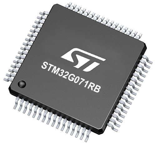
Architecture
ARM Cortex-M0
MCU Memory (KB)
128
Silicon Vendor
STMicroelectronics
Pin count
64
RAM (Bytes)
36864
You complete me!
Accessories
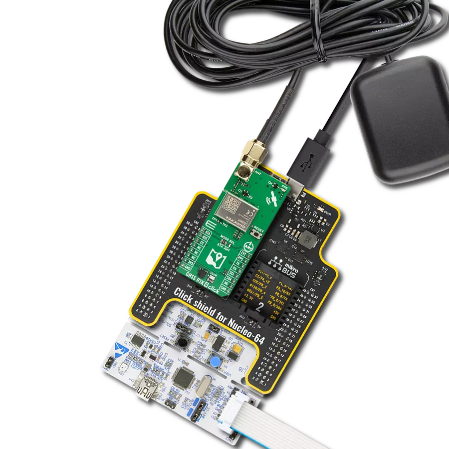
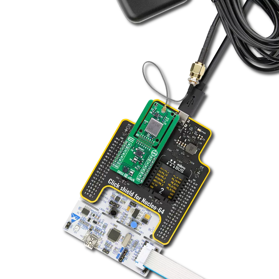
Click Shield for Nucleo-64 comes equipped with two proprietary mikroBUS™ sockets, allowing all the Click board™ devices to be interfaced with the STM32 Nucleo-64 board with no effort. This way, Mikroe allows its users to add any functionality from our ever-growing range of Click boards™, such as WiFi, GSM, GPS, Bluetooth, ZigBee, environmental sensors, LEDs, speech recognition, motor control, movement sensors, and many more. More than 1537 Click boards™, which can be stacked and integrated, are at your disposal. The STM32 Nucleo-64 boards are based on the microcontrollers in 64-pin packages, a 32-bit MCU with an ARM Cortex M4 processor operating at 84MHz, 512Kb Flash, and 96KB SRAM, divided into two regions where the top section represents the ST-Link/V2 debugger and programmer while the bottom section of the board is an actual development board. These boards are controlled and powered conveniently through a USB connection to program and efficiently debug the Nucleo-64 board out of the box, with an additional USB cable connected to the USB mini port on the board. Most of the STM32 microcontroller pins are brought to the IO pins on the left and right edge of the board, which are then connected to two existing mikroBUS™ sockets. This Click Shield also has several switches that perform functions such as selecting the logic levels of analog signals on mikroBUS™ sockets and selecting logic voltage levels of the mikroBUS™ sockets themselves. Besides, the user is offered the possibility of using any Click board™ with the help of existing bidirectional level-shifting voltage translators, regardless of whether the Click board™ operates at a 3.3V or 5V logic voltage level. Once you connect the STM32 Nucleo-64 board with our Click Shield for Nucleo-64, you can access hundreds of Click boards™, working with 3.3V or 5V logic voltage levels.

Used MCU Pins
mikroBUS™ mapper
Take a closer look
Click board™ Schematic

Step by step
Project assembly
Start by selecting your development board and Click board™. Begin with the Nucleo 64 with STM32G071RB MCU as your development board.


Software Support
Library Description
This library contains API for Nano GPS Click driver.
Key functions:
nanogps_generic_parser- Generic parser functionnanogps_generic_read- Generic read functionnanogps_module_wakeup- Wake-up module.
Open Source
Code example
The complete application code and a ready-to-use project are available through the NECTO Studio Package Manager for direct installation in the NECTO Studio. The application code can also be found on the MIKROE GitHub account.
/*!
 * \file
 * \brief Nanogps Click example
 *
 * # Description
 * This example reads and processes data from Nano GPS Click.
 *
 * The demo application is composed of two sections :
 *
 * ## Application Init
 * Initializes driver and wake-up module.
 *
 * ## Application Task
 * Reads the received data and parses it.
 *
 * ## Additional Function
 * - nanogps_process ( ) - The general process of collecting data the module sends.
 *
 * @note
 * Depending on the environmental conditions and the satellites availability
 * it may take some time for the module to receive the position fix.
 *
 * \author MikroE Team
 *
 */
// ------------------------------------------------------------------- INCLUDES

#include "board.h"
#include "log.h"
#include "nanogps.h"
#include "string.h"

#define PROCESS_COUNTER 15
#define PROCESS_RX_BUFFER_SIZE 600
#define PROCESS_PARSER_BUFFER_SIZE 600

// ------------------------------------------------------------------ VARIABLES

static nanogps_t nanogps;
static log_t logger;

static char current_parser_buf[ PROCESS_PARSER_BUFFER_SIZE ];

// ------------------------------------------------------- ADDITIONAL FUNCTIONS

static void nanogps_process ( void )
{
    int32_t rsp_size;
    uint16_t rsp_cnt = 0;

    char uart_rx_buffer[ PROCESS_RX_BUFFER_SIZE ] = { 0 };
    uint16_t check_buf_cnt;
    uint8_t process_cnt = PROCESS_COUNTER;

    // Clear parser buffer
    memset( current_parser_buf, 0 , PROCESS_PARSER_BUFFER_SIZE );

    while( process_cnt != 0 )
    {
        rsp_size = nanogps_generic_read( &nanogps, &uart_rx_buffer, PROCESS_RX_BUFFER_SIZE );

        if ( rsp_size > 0 )
        {
            // Validation of the received data
            for ( check_buf_cnt = 0; check_buf_cnt < rsp_size; check_buf_cnt++ )
            {
                if ( uart_rx_buffer[ check_buf_cnt ] == 0 )
                {
                    uart_rx_buffer[ check_buf_cnt ] = 13;
                }
            }

            // Storages data in parser buffer
            rsp_cnt += rsp_size;
            if ( rsp_cnt < PROCESS_PARSER_BUFFER_SIZE )
            {
                strncat( current_parser_buf, uart_rx_buffer, rsp_size );
            }
            // Clear RX buffer
            memset( uart_rx_buffer, 0, PROCESS_RX_BUFFER_SIZE );
        }
        else
        {
            process_cnt--;

            // Process delay
            Delay_100ms( );
        }
    }
}

static void parser_application ( char *rsp )
{
    char element_buf[ 200 ] = { 0 };

    log_printf( &logger, "\r\n-----------------------\r\n" );
    nanogps_generic_parser( rsp, NANOGPS_NEMA_GPGGA, NANOGPS_GPGGA_LATITUDE, element_buf );
    if ( strlen( element_buf ) > 0 )
    {
        log_printf( &logger, "Latitude:  %.2s degrees, %s minutes \r\n", element_buf, &element_buf[ 2 ] );
        nanogps_generic_parser( rsp, NANOGPS_NEMA_GPGGA, NANOGPS_GPGGA_LONGITUDE, element_buf );
        log_printf( &logger, "Longitude:  %.3s degrees, %s minutes \r\n", element_buf, &element_buf[ 3 ] );
        memset( element_buf, 0, sizeof( element_buf ) );
        nanogps_generic_parser( rsp, NANOGPS_NEMA_GPGGA, NANOGPS_GPGGA_ALTITUDE, element_buf );
        log_printf( &logger, "Altitude: %s m", element_buf );
    }
    else
    {
        log_printf( &logger, "Waiting for the position fix..." );
    }
}

// ------------------------------------------------------ APPLICATION FUNCTIONS

void application_init ( void )
{
    log_cfg_t log_cfg;
    nanogps_cfg_t cfg;

    /**
     * Logger initialization.
     * Default baud rate: 115200
     * Default log level: LOG_LEVEL_DEBUG
     * @note If USB_UART_RX and USB_UART_TX
     * are defined as HAL_PIN_NC, you will
     * need to define them manually for log to work.
     * See @b LOG_MAP_USB_UART macro definition for detailed explanation.
     */
    LOG_MAP_USB_UART( log_cfg );
    log_init( &logger, &log_cfg );
    log_info( &logger, "---- Application Init ----" );

    //  Click initialization.

    nanogps_cfg_setup( &cfg );
    NANOGPS_MAP_MIKROBUS( cfg, MIKROBUS_1 );
    nanogps_init( &nanogps, &cfg );

    nanogps_module_wakeup( &nanogps );
}

void application_task ( void )
{
    nanogps_process(  );
    parser_application( current_parser_buf );
}

int main ( void )
{
    /* Do not remove this line or clock might not be set correctly. */
    #ifdef PREINIT_SUPPORTED
    preinit();
    #endif

    application_init( );

    for ( ; ; )
    {
        application_task( );
    }

    return 0;
}


// ------------------------------------------------------------------------ END
Additional Support
Resources
Category:GPS/GNSS