Transform device-to-cloud communication with NTP5332 and STM32F103RB
NFC forum-compliant I2C bridge
Published Oct 08, 2024
Click board™
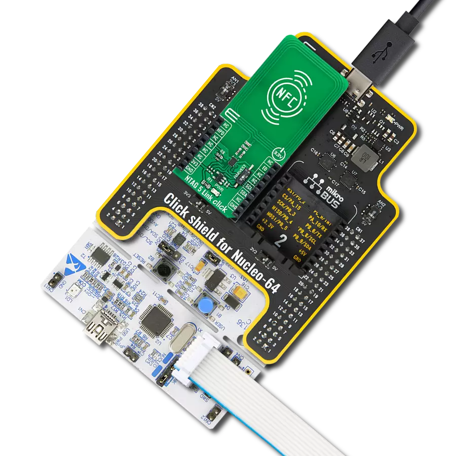
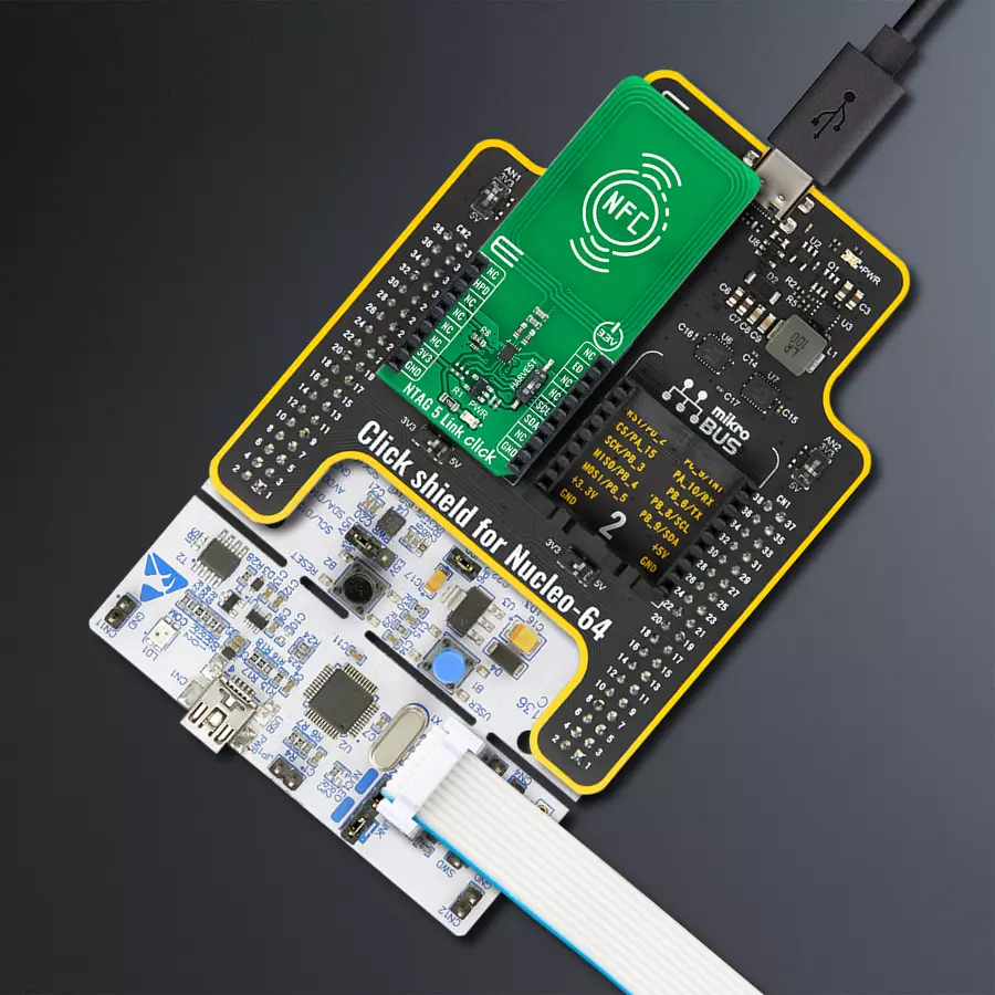
NTAG 5 Link Click
Dev. board
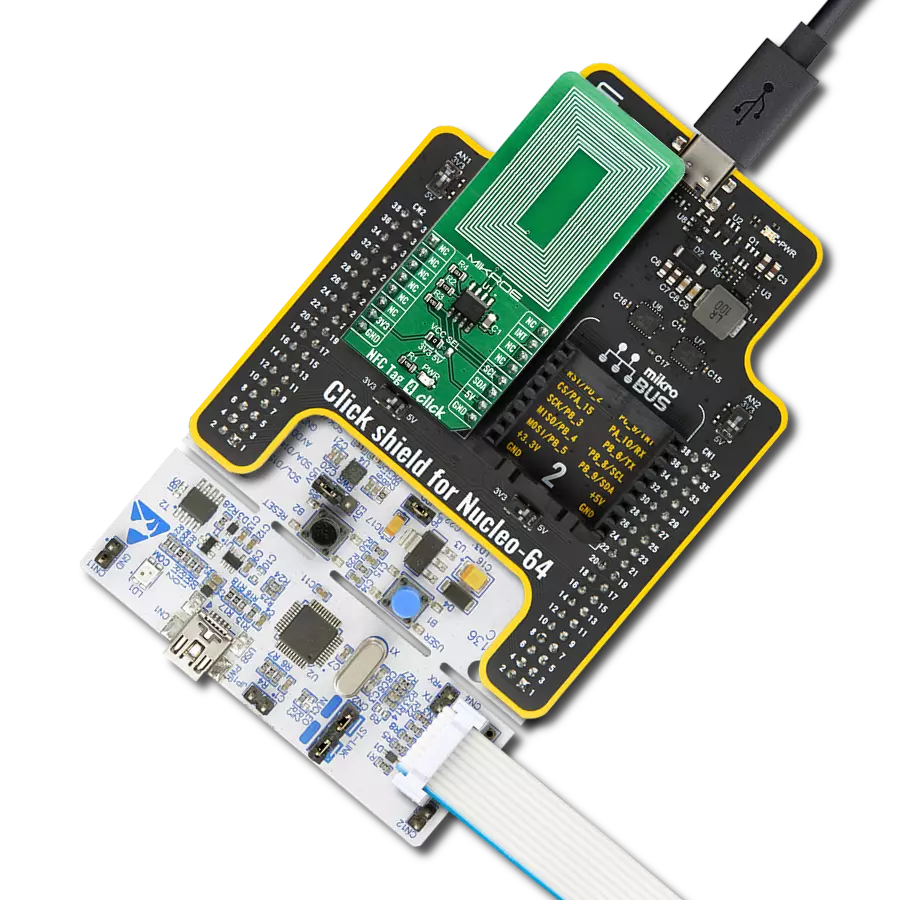
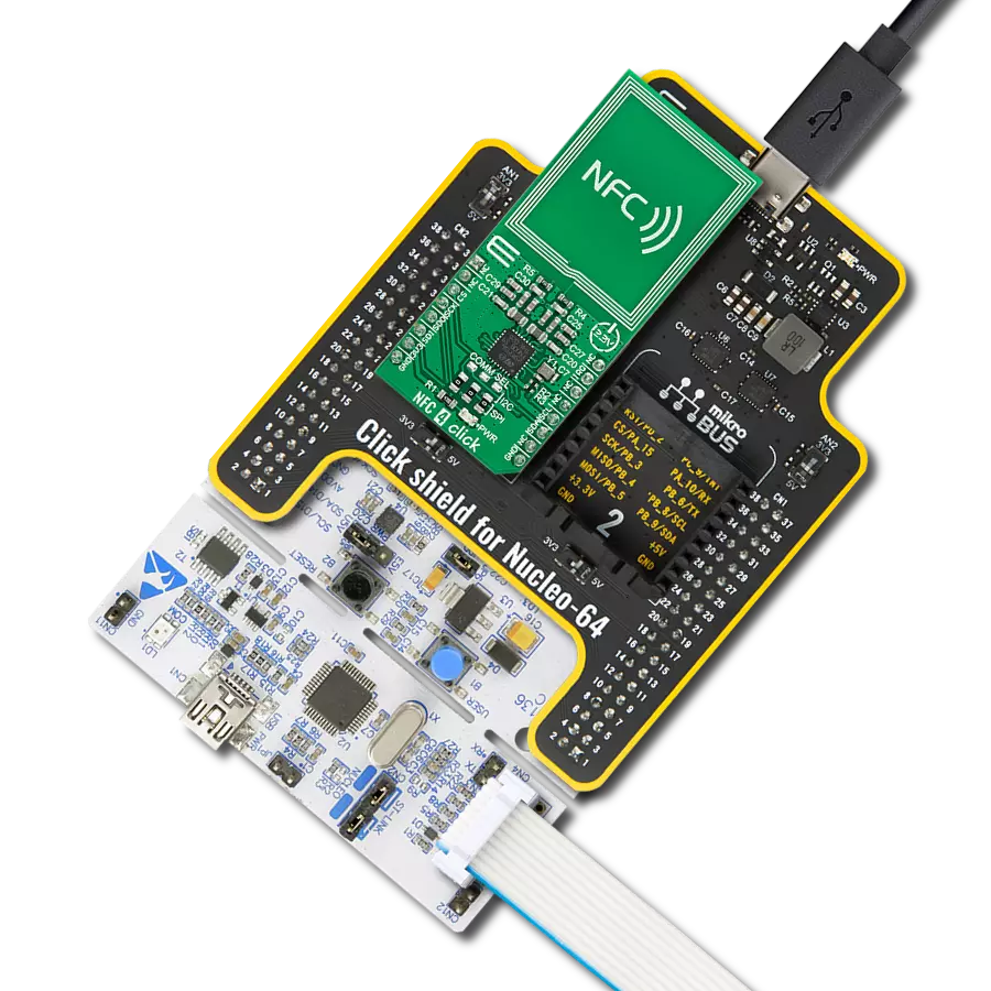
Nucleo 64 with STM32F103RB MCU
Compiler
NECTO Studio
MCU
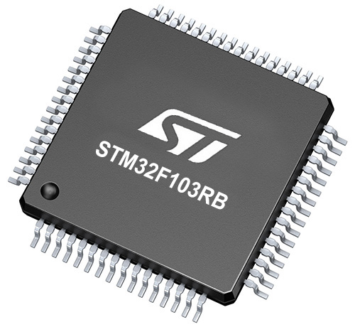
STM32F103RB
Experience the future-proof security with thishighly integrated NFC solution, forging a standard-based link from device to cloud
A
A
Hardware Overview
How does it work?
NTAG 5 Link Click is based on the NTP5332, a highly integrated NFC IC optimized for sensor-driven applications that act as a bridge between an NFC-enabled device and any I2C slave from NXP Semiconductors. This highly integrated NFC IC creates a secure, standard-based link from the device to the cloud in a future-proof way to address and even power sensors. Operating at 13.56 MHz, the NTP5332 is an NFC Forum Type 5 Tag, which can be read and written by an NFC-enabled device at close range and an ISO/IEC 15693-enabled industrial reader over a more extended range (>60cm). With NTAG 5 Link, the device can connect to the cloud with a single tap. The connection uses an NFC Forum-compliant data exchange mechanism involving SRAM to ensure interoperable data transfers. Also, it offers 2048 bytes of memory divided into three areas where each area can use a different protection level, varying from no protection to 32-/64-bit password-protected read/write access or up to 128-bit-AES mutual authentication protected read/write access. The NTAG 5 Link comes with pre-programmed proof-of-origin functionality to verify
authenticity. The ECC-based originality signature can be reprogrammed or locked by the customer through its registers. This Click board™ communicates with MCU using the standard I2C 2-Wire interface to read data and configure settings, supporting Standard Mode operation with a clock frequency of 100kHz and Fast Mode up to 400kHz. The NTP5332 also offers a transparent I2C master mode, for example, to read sensors without a microcontroller. The RF interface initiates an I2C Master communication, which can trigger a read or write transaction to an external I2C slave. Alongside this feature, an integrated SRAM is used as intermediate data storage. Session registers reflect the status of the I2C Master transaction. Therefore an RF reader has to poll for the status bits related to I2C Master to know the status of the current I2C transaction. The NTAG 5 Link can also operate as a standalone solution by drawing power from the NFC field of an NFC device. It supports an energy harvesting feature, activated by an onboard switch marked as HARVEST, which means it can supply power to other components in the system, in this case,
to supply the NTP5332. NTAG 5 Link can provide a fixed configurable voltage level of 1.8V, 2.4V, or 3V, selectable through register configuration when sufficient energy is available. In addition, this Click board™ can be placed in a hard power-down mode by setting the HPD pin routed on the RST pin of the mikroBUS™ socket. Besides, it also has an event detection and field detection functionality that defines the ED pin's behavior routed on the INT pin of the mikroBUS™ socket. This pin's behavior depends on various events such as the presence/absence of the NFC field, arbiter locked/unlocked EEPROM to NFC interface, Write/Read command ongoing, and more. This Click board™ can only be operated with a 3.3V logic voltage level. The board must perform appropriate logic voltage level conversion before using MCUs with different logic levels. However, the Click board™ comes equipped with a library containing functions and an example code that can be used as a reference for further development.


Features overview
Development board
Nucleo-64 with STM32F103RB MCU offers a cost-effective and adaptable platform for developers to explore new ideas and prototype their designs. This board harnesses the versatility of the STM32 microcontroller, enabling users to select the optimal balance of performance and power consumption for their projects. It accommodates the STM32 microcontroller in the LQFP64 package and includes essential components such as a user LED, which doubles as an ARDUINO® signal, alongside user and reset push-buttons, and a 32.768kHz crystal oscillator for precise timing operations. Designed with expansion and flexibility in mind, the Nucleo-64 board features an ARDUINO® Uno V3 expansion connector and ST morpho extension pin
headers, granting complete access to the STM32's I/Os for comprehensive project integration. Power supply options are adaptable, supporting ST-LINK USB VBUS or external power sources, ensuring adaptability in various development environments. The board also has an on-board ST-LINK debugger/programmer with USB re-enumeration capability, simplifying the programming and debugging process. Moreover, the board is designed to simplify advanced development with its external SMPS for efficient Vcore logic supply, support for USB Device full speed or USB SNK/UFP full speed, and built-in cryptographic features, enhancing both the power efficiency and security of projects. Additional connectivity is
provided through dedicated connectors for external SMPS experimentation, a USB connector for the ST-LINK, and a MIPI® debug connector, expanding the possibilities for hardware interfacing and experimentation. Developers will find extensive support through comprehensive free software libraries and examples, courtesy of the STM32Cube MCU Package. This, combined with compatibility with a wide array of Integrated Development Environments (IDEs), including IAR Embedded Workbench®, MDK-ARM, and STM32CubeIDE, ensures a smooth and efficient development experience, allowing users to fully leverage the capabilities of the Nucleo-64 board in their projects.

Microcontroller Overview
MCU Card / MCU
Architecture
ARM Cortex-M3
MCU Memory (KB)
128
Silicon Vendor
STMicroelectronics
Pin count
64
RAM (Bytes)
20480
You complete me!
Accessories
Click Shield for Nucleo-64 comes equipped with two proprietary mikroBUS™ sockets, allowing all the Click board™ devices to be interfaced with the STM32 Nucleo-64 board with no effort. This way, Mikroe allows its users to add any functionality from our ever-growing range of Click boards™, such as WiFi, GSM, GPS, Bluetooth, ZigBee, environmental sensors, LEDs, speech recognition, motor control, movement sensors, and many more. More than 1537 Click boards™, which can be stacked and integrated, are at your disposal. The STM32 Nucleo-64 boards are based on the microcontrollers in 64-pin packages, a 32-bit MCU with an ARM Cortex M4 processor operating at 84MHz, 512Kb Flash, and 96KB SRAM, divided into two regions where the top section represents the ST-Link/V2 debugger and programmer while the bottom section of the board is an actual development board. These boards are controlled and powered conveniently through a USB connection to program and efficiently debug the Nucleo-64 board out of the box, with an additional USB cable connected to the USB mini port on the board. Most of the STM32 microcontroller pins are brought to the IO pins on the left and right edge of the board, which are then connected to two existing mikroBUS™ sockets. This Click Shield also has several switches that perform functions such as selecting the logic levels of analog signals on mikroBUS™ sockets and selecting logic voltage levels of the mikroBUS™ sockets themselves. Besides, the user is offered the possibility of using any Click board™ with the help of existing bidirectional level-shifting voltage translators, regardless of whether the Click board™ operates at a 3.3V or 5V logic voltage level. Once you connect the STM32 Nucleo-64 board with our Click Shield for Nucleo-64, you can access hundreds of Click boards™, working with 3.3V or 5V logic voltage levels.

Used MCU Pins
mikroBUS™ mapper
Take a closer look
Click board™ Schematic

Step by step
Project assembly
Start by selecting your development board and Click board™. Begin with the Nucleo 64 with STM32F103RB MCU as your development board.


Track your results in real time
Application Output
1. Application Output - In Debug mode, the 'Application Output' window enables real-time data monitoring, offering direct insight into execution results. Ensure proper data display by configuring the environment correctly using the provided tutorial.

2. UART Terminal - Use the UART Terminal to monitor data transmission via a USB to UART converter, allowing direct communication between the Click board™ and your development system. Configure the baud rate and other serial settings according to your project's requirements to ensure proper functionality. For step-by-step setup instructions, refer to the provided tutorial.

3. Plot Output - The Plot feature offers a powerful way to visualize real-time sensor data, enabling trend analysis, debugging, and comparison of multiple data points. To set it up correctly, follow the provided tutorial, which includes a step-by-step example of using the Plot feature to display Click board™ readings. To use the Plot feature in your code, use the function: plot(*insert_graph_name*, variable_name);. This is a general format, and it is up to the user to replace 'insert_graph_name' with the actual graph name and 'variable_name' with the parameter to be displayed.

Software Support
Library Description
This library contains API for NTAG 5 Link Click driver.
Key functions:
ntag5link_write_ndef_uri_recordThis function writes specific NDEF URI record to the memory address specified with NTAG5LINK_NDEF_MESSAGE_START_ADDRESS macro.ntag5link_write_message_to_memoryThis function writes a specified number of data bytes to the user memory starting from block_addr.ntag5link_read_message_from_memoryThis function reads a specified number of data bytes from the user memory starting from @b block_addr.
Open Source
Code example
The complete application code and a ready-to-use project are available through the NECTO Studio Package Manager for direct installation in the NECTO Studio. The application code can also be found on the MIKROE GitHub account.
/*!
 * @file main.c
 * @brief NTAG5Link Click example
 *
 * # Description
 * This example demonstrates the use of NTAG 5 Link Click board by programming the
 * specified NDEF URI record to the memory, and showing the memory read/write feature.
 *
 * The demo application is composed of two sections :
 *
 * ## Application Init
 * Initializes the driver and logger and performs the Click default configuration which
 * enables the device and formats its user memory. After that it programs the specified
 * NDEF URI record to the memory.
 *
 * ## Application Task
 * Writes a desired number of data bytes to the memory and verifies that it is written
 * correctly by reading from the same memory location and displaying the memory content
 * on the USB UART approximately every 5 seconds.
 *
 * @author Stefan Filipovic
 *
 */

#include "board.h"
#include "log.h"
#include "ntag5link.h"

/**
 * URL to store to memory as NDEF URI record
 */
#define URI_DATA                "www.mikroe.com/ntag-5-link-click"

/**
 * Starting block address to where the text message will be stored
 * Must be > ( NTAG5LINK_NDEF_MESSAGE_START_ADDRESS + sizeof ( URI_DATA ) / NTAG5LINK_MEMORY_BLOCK_SIZE + 3 )
 * to avoid overwriting NDEF URI record.
 */
#define TEXT_MESSAGE_ADDRESS    0x0040

/**
 * Text message content that will be stored to memory
 */
#define TEXT_MESSAGE            "MikroE - NTAG 5 Link Click"

static ntag5link_t ntag5link;
static log_t logger;

void application_init ( void )
{
    log_cfg_t log_cfg;  /**< Logger config object. */
    ntag5link_cfg_t ntag5link_cfg;  /**< Click config object. */

    /**
     * Logger initialization.
     * Default baud rate: 115200
     * Default log level: LOG_LEVEL_DEBUG
     * @note If USB_UART_RX and USB_UART_TX
     * are defined as HAL_PIN_NC, you will
     * need to define them manually for log to work.
     * See @b LOG_MAP_USB_UART macro definition for detailed explanation.
     */
    LOG_MAP_USB_UART( log_cfg );
    log_init( &logger, &log_cfg );
    log_info( &logger, " Application Init " );

    // Click initialization.
    ntag5link_cfg_setup( &ntag5link_cfg );
    NTAG5LINK_MAP_MIKROBUS( ntag5link_cfg, MIKROBUS_1 );
    if ( I2C_MASTER_ERROR == ntag5link_init( &ntag5link, &ntag5link_cfg ) )
    {
        log_error( &logger, " Communication init." );
        for ( ; ; );
    }

    if ( NTAG5LINK_ERROR == ntag5link_default_cfg ( &ntag5link ) )
    {
        log_error( &logger, " Default configuration." );
        for ( ; ; );
    }

    if ( NTAG5LINK_OK == ntag5link_write_ndef_uri_record ( &ntag5link, NTAG5LINK_URI_PREFIX_4,
                                                           URI_DATA, strlen ( URI_DATA ) ) )
    {
        log_printf( &logger, " NDEF URI record \"https://%s\" has been written\r\n", ( char * ) URI_DATA );
    }

    log_info( &logger, " Application Task " );
}

void application_task ( void )
{
    uint8_t message_buf[ 100 ] = { 0 };
    if ( NTAG5LINK_OK == ntag5link_write_message_to_memory ( &ntag5link,
                                                             TEXT_MESSAGE_ADDRESS,
                                                             TEXT_MESSAGE,
                                                             strlen ( TEXT_MESSAGE ) ) )
    {
        log_printf( &logger, " \"%s\" has been written to memory address 0x%.4X \r\n",
                    ( char * ) TEXT_MESSAGE, ( uint16_t ) TEXT_MESSAGE_ADDRESS );
    }
    if ( NTAG5LINK_OK == ntag5link_read_message_from_memory ( &ntag5link,
                                                              TEXT_MESSAGE_ADDRESS,
                                                              message_buf,
                                                              strlen ( TEXT_MESSAGE ) ) )
    {
        log_printf( &logger, " \"%s\" has been read from memory address 0x%.4X \r\n\n",
                    message_buf, ( uint16_t ) TEXT_MESSAGE_ADDRESS );
    }
    Delay_ms ( 1000 );
    Delay_ms ( 1000 );
    Delay_ms ( 1000 );
    Delay_ms ( 1000 );
    Delay_ms ( 1000 );
}

int main ( void )
{
    /* Do not remove this line or clock might not be set correctly. */
    #ifdef PREINIT_SUPPORTED
    preinit();
    #endif

    application_init( );

    for ( ; ; )
    {
        application_task( );
    }

    return 0;
}

// ------------------------------------------------------------------------ END
Additional Support
Resources
Category:RFID/NFC