Ensure error-free and robust RS485 data transfer in harsh environments using MAX3471 and STM32F103RB
Simplify, optimize, transform: The future of data communication!

Published Oct 08, 2024
Click board™
RS485 2 Click
Dev. board
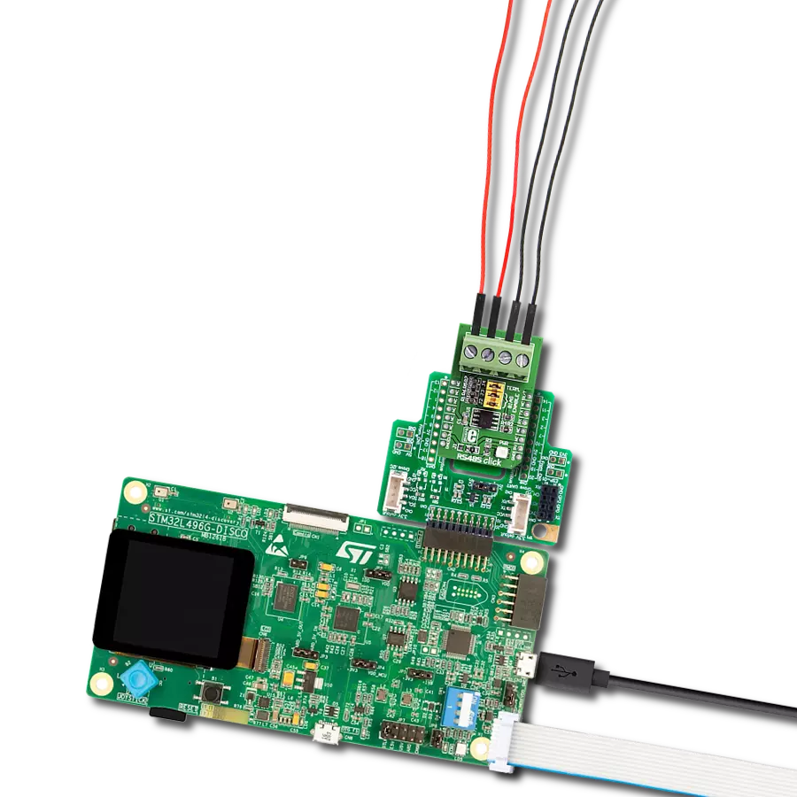
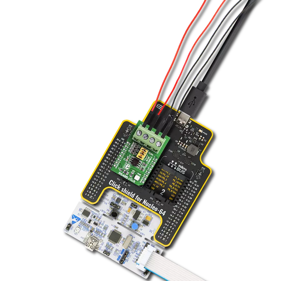
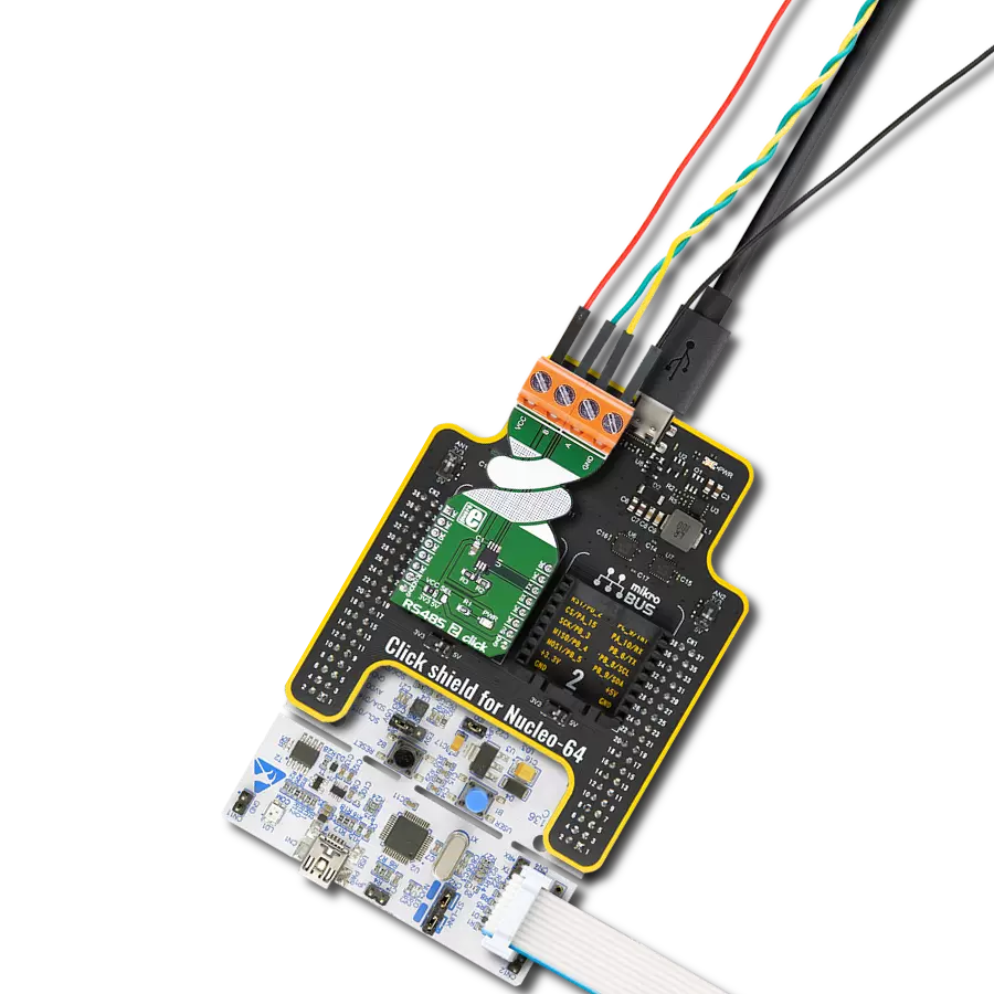
Nucleo 64 with STM32F103RB MCU
Compiler
NECTO Studio
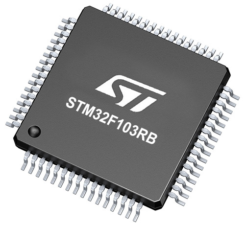
MCU
STM32F103RB
Our solution seamlessly transforms UART signals to RS485, empowering industrial automation systems with faster and more reliable data communication.
A
A
Hardware Overview
How does it work?
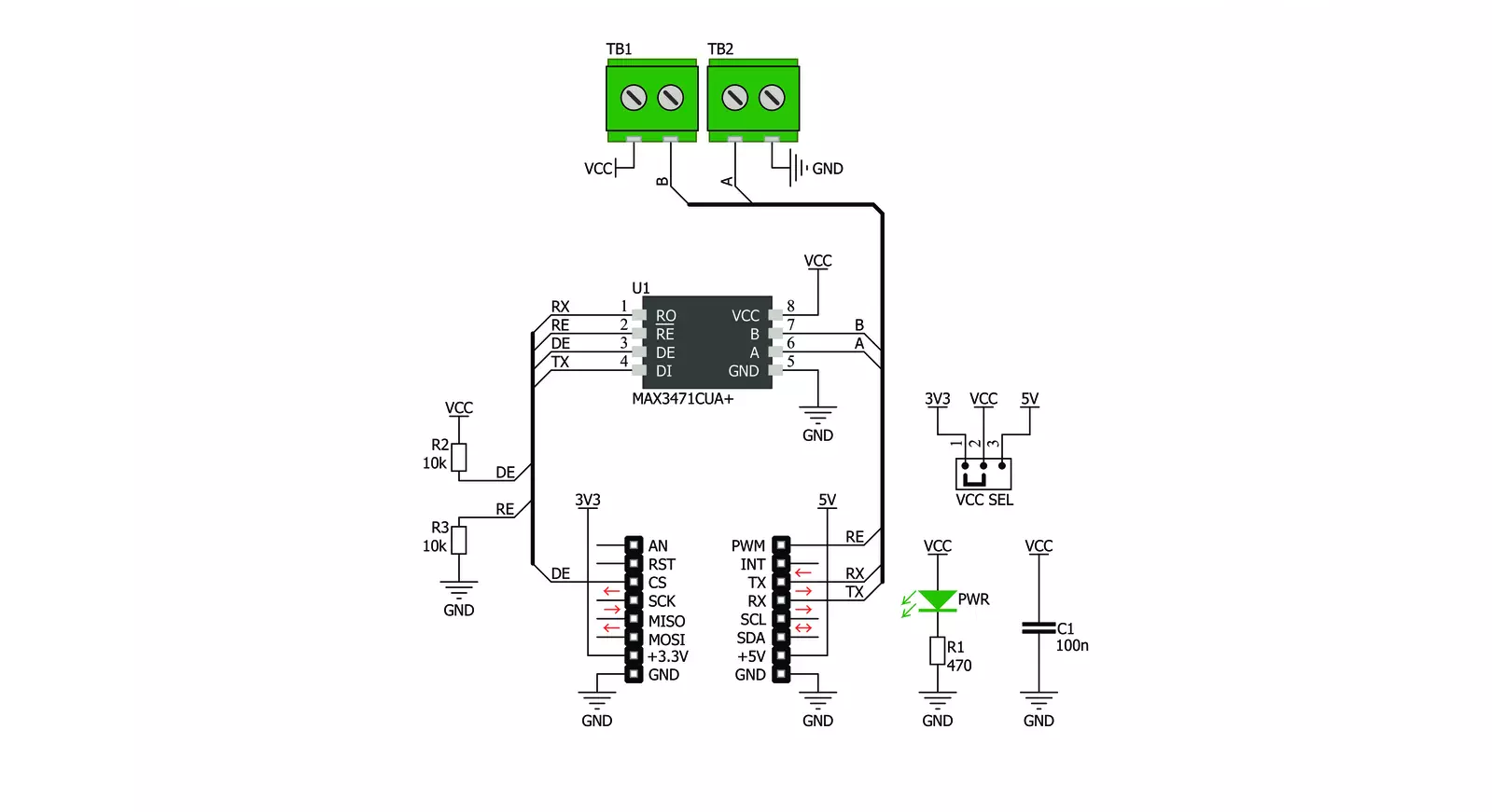
RS485 2 Click is based on the MAX3471, an RS-422/485, half-duplex, differential transceiver for battery-powered systems, from Analog Devices. This click is intended to be used as a physical layer device, often referred to as PHY, providing physical interfacing of the MCU TTL level UART lines with the RS422/485 bus. It is well suited for transmitting smaller blocks of data over long distances, using a shielded differential pair, for both TX and RX signals, allowing for half-duplex asynchronous communication. The MAX3471 transceiver consists of a separate driver and receiver sections, with Driver Enable and Receiver Enable pins (#RE and DE), used to enable appropriate sections. Driver section is used to drive the RS422/485 bus with the signal received on the UART RX line labeled as RO on the IC, while the receiver section returns data from the bus back to the MCU via the UART TX line, labeled as DI on the IC in the schematics. RS422/485 standard only specifies electrical characteristics of the transmitter and the receiver. It does not specify or recommend any communications protocol, only the physical layer. The top layer communication protocol of choice can be used, such as the MODBUS or similar protocols. Therefore RS485 2 click offers UART RX and TX pins, routed to the appropriate mikroBUS™ TX and RX UART pins. These pins are used by the MCU to send data to the RS485 bus, in a form determined by the user protocol. Additional DE and RE pins are routed to the mikroBUS™ CS and PWM pin respectively. These pins are labeled on
the Click board™ as DE and RE, the same as on the IC itself. Pull-up and pull-down are used to determine states on these pins when they are left floating. MAX3471 IC allows data rates up to 64kbps. In general, the maximal transfer speed is determined by the bus length: longer bus lines will result in less transfer speed. The RS485/422 bus needs to be terminated with the resistor on both ends, which is equal to the characteristic impedance of the used cable, in order to prevent line reflections. However, the MAX3471 IC features a reduced slew rate on its driver outputs, resulting with slower speed, but with far more robust signal at the same time, which is immune to EMI and other types of interferences that appear on long lines or connection stubs (unterminated parts of the bus). This IC is also able to work on the unterminated bus, commonly used in low speed and low power systems. The RS-485 standard specifies that a compliant driver must be able to drive 32 unit loads (UL), where 1 unit load represents a load impedance of approximately 12 kΩ. Since the MAX3471 IC device is 1/8 UL, up to 256 such receivers can be supported by a single driver. In cases when the RS485/422 bus voltage is close to 2.5V, the device is able to drive up to 8 loads, which means that it can drive up to 64 receivers. As the bus voltage rises, more drivers can be added, so that for 5V the device can drive the number of devices specified by the standard. There are situations on the RS485/422 bus, which might lead to a differential voltage which can
increase the current which runs through the driver output. This state is known as the bus contention, and it commonly appears during the initialization, bus fault conditions, or with multiple nodes, which have their drivers active at the same time. The MAX3471 IC provides driver output protection, which limits this current and prevents damage to the driver output stage. The MAX3471 receiver employs input filtering and input hysteresis to enhance noise immunity when differential signals have very slow rise and fall times. MAX3471 IC features a true fail-safe receiver input, which guarantees a logic HIGH receiver output in cases when the receiver inputs are open or shorted, or when they are connected to a terminated transmission line with all drivers disabled. There is one 4-pole screw terminal on board (VCC, RX, TX, GND) for connecting RS422/485 bus twisted pair cable, along with the GND and VCC. The jumper labeled as VCC SEL is used to set the operating voltage of the Click board™ to either 3.3V or 5V. GND and VCC rails can be used to provide the power supply for another node. Note that the VCC terminal is directly routed to either 3.3V or 5V rail of the mikroBUS™, depending on the VCC SEL jumper position. MikroElektronika provides a library that contains functions compatible with the MikroElektronika compilers, which can be used for working with the RS485 2 Click. The library also contains an example application, which demonstrates their use. This example application can be used as a reference for custom designs.


Features overview
Development board
Nucleo-64 with STM32F103RB MCU offers a cost-effective and adaptable platform for developers to explore new ideas and prototype their designs. This board harnesses the versatility of the STM32 microcontroller, enabling users to select the optimal balance of performance and power consumption for their projects. It accommodates the STM32 microcontroller in the LQFP64 package and includes essential components such as a user LED, which doubles as an ARDUINO® signal, alongside user and reset push-buttons, and a 32.768kHz crystal oscillator for precise timing operations. Designed with expansion and flexibility in mind, the Nucleo-64 board features an ARDUINO® Uno V3 expansion connector and ST morpho extension pin
headers, granting complete access to the STM32's I/Os for comprehensive project integration. Power supply options are adaptable, supporting ST-LINK USB VBUS or external power sources, ensuring adaptability in various development environments. The board also has an on-board ST-LINK debugger/programmer with USB re-enumeration capability, simplifying the programming and debugging process. Moreover, the board is designed to simplify advanced development with its external SMPS for efficient Vcore logic supply, support for USB Device full speed or USB SNK/UFP full speed, and built-in cryptographic features, enhancing both the power efficiency and security of projects. Additional connectivity is
provided through dedicated connectors for external SMPS experimentation, a USB connector for the ST-LINK, and a MIPI® debug connector, expanding the possibilities for hardware interfacing and experimentation. Developers will find extensive support through comprehensive free software libraries and examples, courtesy of the STM32Cube MCU Package. This, combined with compatibility with a wide array of Integrated Development Environments (IDEs), including IAR Embedded Workbench®, MDK-ARM, and STM32CubeIDE, ensures a smooth and efficient development experience, allowing users to fully leverage the capabilities of the Nucleo-64 board in their projects.

Microcontroller Overview
MCU Card / MCU
Architecture
ARM Cortex-M3
MCU Memory (KB)
128
Silicon Vendor
STMicroelectronics
Pin count
64
RAM (Bytes)
20480
You complete me!
Accessories
Click Shield for Nucleo-64 comes equipped with two proprietary mikroBUS™ sockets, allowing all the Click board™ devices to be interfaced with the STM32 Nucleo-64 board with no effort. This way, Mikroe allows its users to add any functionality from our ever-growing range of Click boards™, such as WiFi, GSM, GPS, Bluetooth, ZigBee, environmental sensors, LEDs, speech recognition, motor control, movement sensors, and many more. More than 1537 Click boards™, which can be stacked and integrated, are at your disposal. The STM32 Nucleo-64 boards are based on the microcontrollers in 64-pin packages, a 32-bit MCU with an ARM Cortex M4 processor operating at 84MHz, 512Kb Flash, and 96KB SRAM, divided into two regions where the top section represents the ST-Link/V2 debugger and programmer while the bottom section of the board is an actual development board. These boards are controlled and powered conveniently through a USB connection to program and efficiently debug the Nucleo-64 board out of the box, with an additional USB cable connected to the USB mini port on the board. Most of the STM32 microcontroller pins are brought to the IO pins on the left and right edge of the board, which are then connected to two existing mikroBUS™ sockets. This Click Shield also has several switches that perform functions such as selecting the logic levels of analog signals on mikroBUS™ sockets and selecting logic voltage levels of the mikroBUS™ sockets themselves. Besides, the user is offered the possibility of using any Click board™ with the help of existing bidirectional level-shifting voltage translators, regardless of whether the Click board™ operates at a 3.3V or 5V logic voltage level. Once you connect the STM32 Nucleo-64 board with our Click Shield for Nucleo-64, you can access hundreds of Click boards™, working with 3.3V or 5V logic voltage levels.

Used MCU Pins
mikroBUS™ mapper
Take a closer look
Click board™ Schematic
Step by step
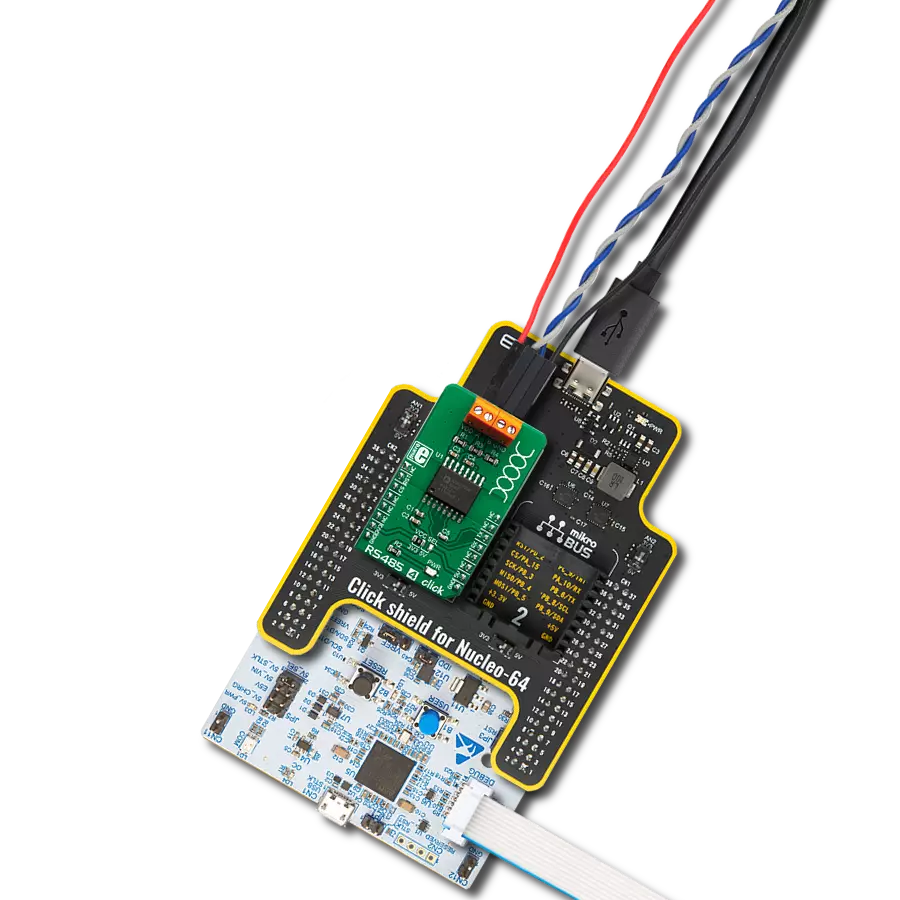
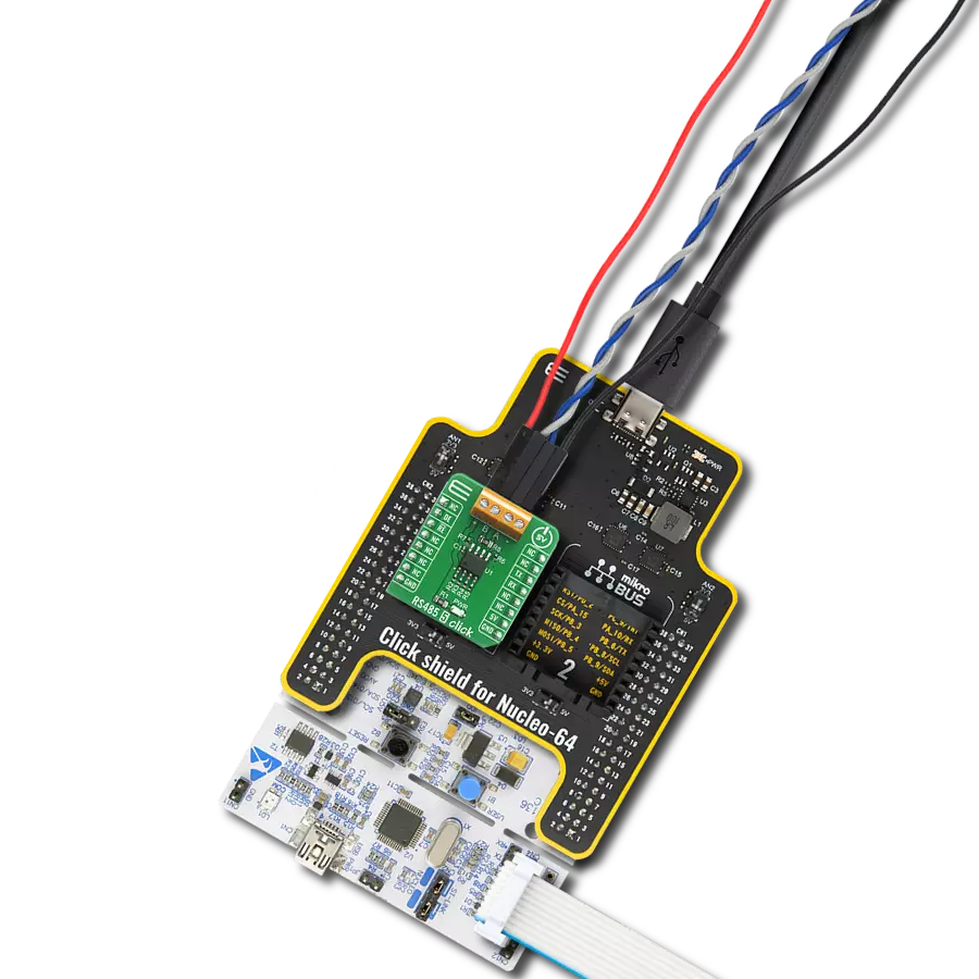
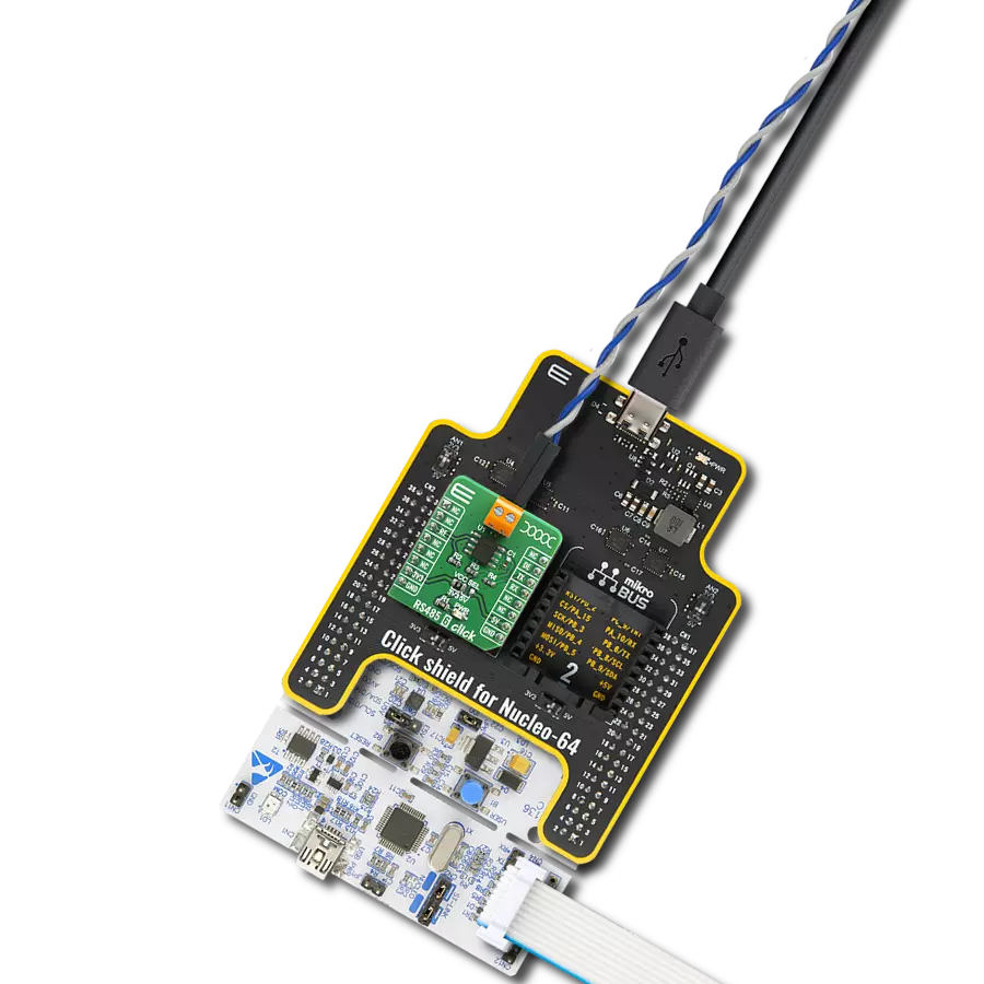
Project assembly
Start by selecting your development board and Click board™. Begin with the Nucleo 64 with STM32F103RB MCU as your development board.


Software Support
Library Description
This library contains API for RS485 2 Click driver.
Key functions:
rs4852_generic_read- Generic read function.rs4852_generic_write- Generic write function.rs4852_set_de_pin- Set DE ( cs ) pin state.
Open Source
Code example
The complete application code and a ready-to-use project are available through the NECTO Studio Package Manager for direct installation in the NECTO Studio. The application code can also be found on the MIKROE GitHub account.
/*!
 * \file
 * \brief Rs4852 Click example
 *
 * # Description
 * This example reads and processes data from RS485 2 Clicks.
 *
 * The demo application is composed of two sections :
 *
 * ## Application Init
 * Initializes the driver and enables the selected mode.
 *
 * ## Application Task
 * Depending on the selected mode, it reads all the received data or sends the desired message
 * every 2 seconds.
 *
 * ## Additional Function
 * - rs4852_process ( ) - The general process of collecting the received data.
 *
 * \author MikroE Team
 *
 */
// ------------------------------------------------------------------- INCLUDES

#include "board.h"
#include "log.h"
#include "rs4852.h"
#include "string.h"

#define PROCESS_RX_BUFFER_SIZE 500

#define TEXT_TO_SEND "MikroE - RS485 2 Click board\r\n"

// #define DEMO_APP_RECEIVER
#define DEMO_APP_TRANSMITTER

// ------------------------------------------------------------------ VARIABLES

static rs4852_t rs4852;
static log_t logger;

// ------------------------------------------------------- ADDITIONAL FUNCTIONS

static void rs4852_process ( void )
{
    int32_t rsp_size;

    char uart_rx_buffer[ PROCESS_RX_BUFFER_SIZE ] = { 0 };
    uint8_t check_buf_cnt;

    rsp_size = rs4852_generic_read( &rs4852, uart_rx_buffer, PROCESS_RX_BUFFER_SIZE );

    if ( rsp_size > 0 )
    {
        for ( uint8_t cnt = 0; cnt < rsp_size; cnt++ )
        {
            log_printf( &logger, "%c", uart_rx_buffer[ cnt ] );
            if ( uart_rx_buffer[ cnt ] == '\n' )
            {
                log_printf( &logger, "--------------------------------\r\n" );
            }
        }
    }
}

// ------------------------------------------------------ APPLICATION FUNCTIONS

void application_init ( void )
{
    log_cfg_t log_cfg;
    rs4852_cfg_t cfg;

    /**
     * Logger initialization.
     * Default baud rate: 115200
     * Default log level: LOG_LEVEL_DEBUG
     * @note If USB_UART_RX and USB_UART_TX
     * are defined as HAL_PIN_NC, you will
     * need to define them manually for log to work.
     * See @b LOG_MAP_USB_UART macro definition for detailed explanation.
     */
    LOG_MAP_USB_UART( log_cfg );
    log_init( &logger, &log_cfg );
    log_info( &logger, "---- Application Init ----" );

    //  Click initialization.

    rs4852_cfg_setup( &cfg );
    RS4852_MAP_MIKROBUS( cfg, MIKROBUS_1 );
    rs4852_init( &rs4852, &cfg );
    Delay_ms ( 100 );

#ifdef DEMO_APP_RECEIVER
    rs4852_set_re_pin( &rs4852, RS4852_ENABLE_RE );
    rs4852_set_de_pin( &rs4852, RS4852_DISABLE_DE );
    log_info( &logger, "---- Receiver mode ----" );
#endif
#ifdef DEMO_APP_TRANSMITTER
    rs4852_set_de_pin( &rs4852, RS4852_ENABLE_DE );
    rs4852_set_re_pin( &rs4852, RS4852_DISABLE_RE );
    log_info( &logger, "---- Transmitter mode ----" );
#endif
    Delay_ms ( 100 );
}

void application_task ( void )
{
#ifdef DEMO_APP_RECEIVER
    rs4852_process( );
#endif

#ifdef DEMO_APP_TRANSMITTER
    rs4852_generic_write( &rs4852, TEXT_TO_SEND, strlen( TEXT_TO_SEND ) );
    log_info( &logger, "---- Data sent ----" );
    Delay_ms ( 1000 );
    Delay_ms ( 1000 );
#endif
}

int main ( void )
{
    /* Do not remove this line or clock might not be set correctly. */
    #ifdef PREINIT_SUPPORTED
    preinit();
    #endif

    application_init( );

    for ( ; ; )
    {
        application_task( );
    }

    return 0;
}

// ------------------------------------------------------------------------ END
Additional Support
Resources
Category:RS485