Create precise time intervals with DS1087L and STM32F031K6
Accurate square wave generator

Published Oct 01, 2024
Click board™
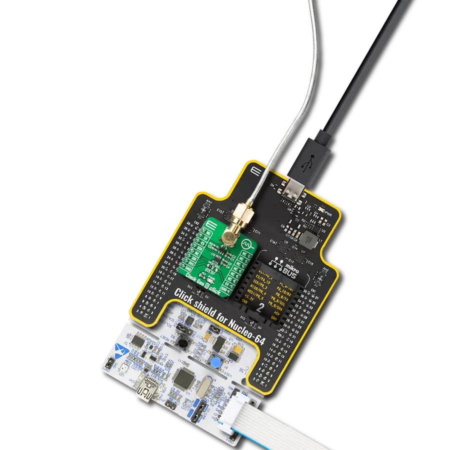
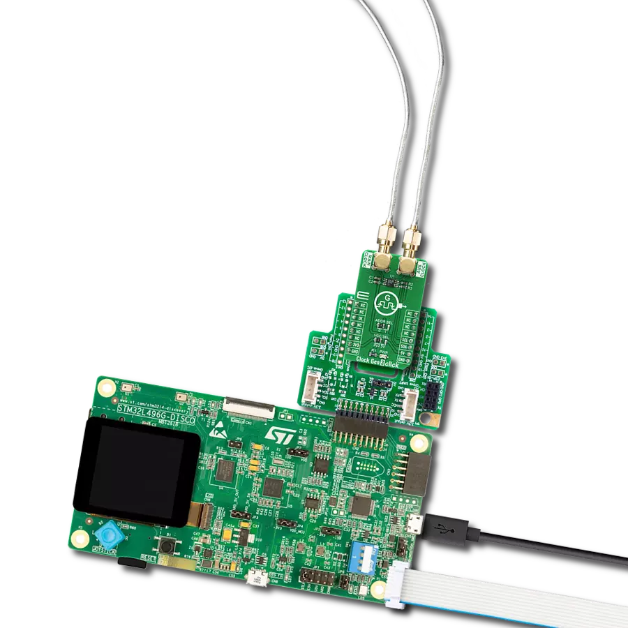
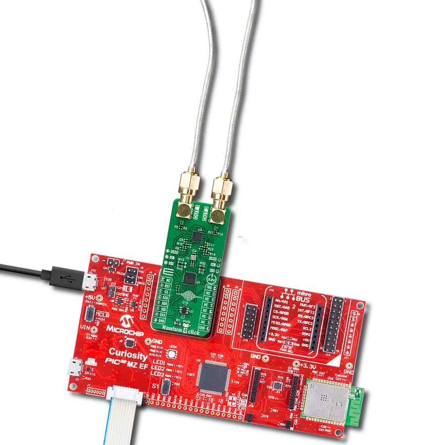
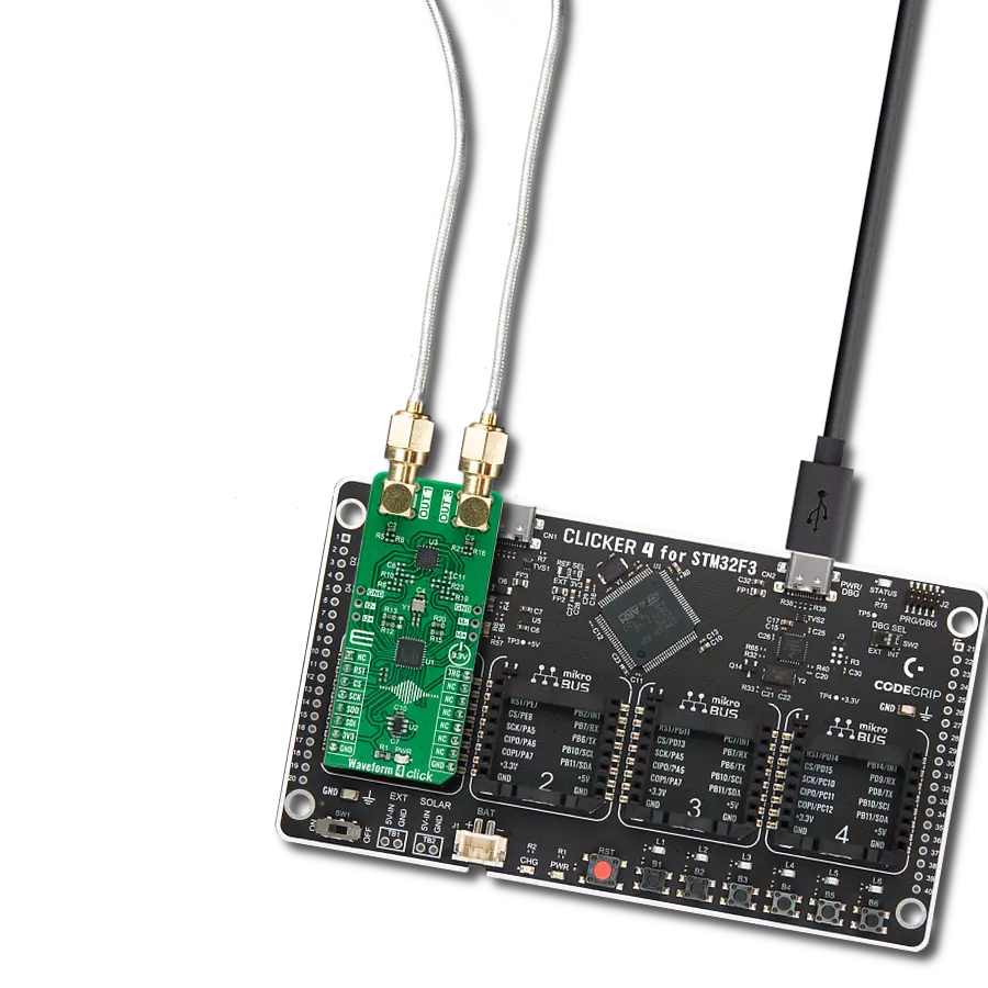
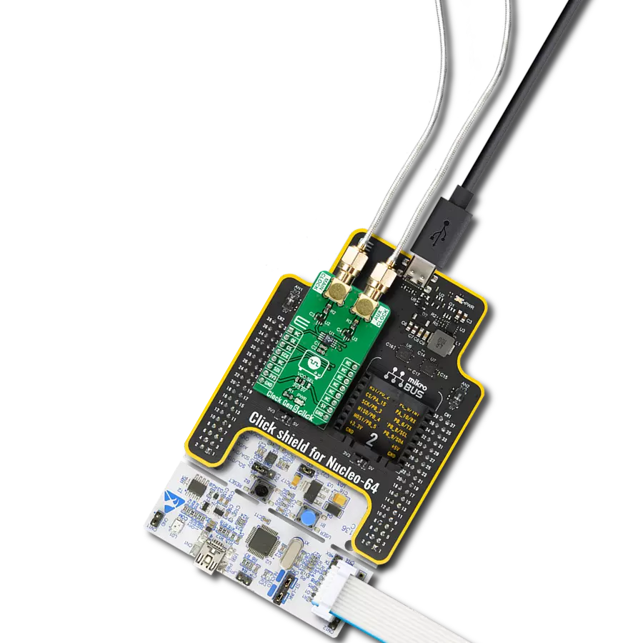
Clock Gen 2 Click
Dev. board
Nucleo 32 with STM32F031K6 MCU
Compiler
NECTO Studio
MCU
STM32F031K6
Elevate your engineering solution with a cutting-edge clock generator, delivering reliable and efficient timing signals
A
A
Hardware Overview
How does it work?
Clock Gen 2 Click is based on the DS1087, a 3.3V spread-spectrum EconOscillator from Analog Devices. This IC is factory-produced with a range of different master clock frequencies, ranging from 33.3 MHz, up to 66.6 MHz, with variable spread spectrum percentages. The IC on the Clock Gen 2 click has the master clock fixed to 66.6 MHz, allowing the frequency range from 260 kHz to 66.6 MHz. This IC uses the clock prescaler from 2 0 to 2 8 to achieve frequencies different from the master frequency. By selecting the spread-spectrum percentage, it is possible to avoid the generation of too much EMI, which otherwise might violate the FCC/IEC regulations. As mentioned, the internal clock frequency that the DS1087 generates is 66.6MHz. The master clock is frequency-modulated by the internal triangle wave generator. The main oscillator frequency can be dithered below the maximum frequency by a selectable ratio. A bit in the prescaler register determines the spread-spectrum dither range, which can be selected between 2% and 4%
under the main clock frequency. The IC pin labeled as SPRD is routed to the mikroBUS™ PWM pin. A logic HIGH level on this pin enables the spread-spectrum function. The DS1087LU is equipped with non-volatile memory locations (EEPROM) to store the content of all the configuration registers. Writing data to the configuration registers can be automatically mirrored to the EEPROM. This is controlled by the Write Control bit (WC). It allows automatically storing data to EEPROM after each register change (WC = 0, default) or storing the config data manually by issuing the WRITE EE command (WC = 1). This feature allows the configuration to be remembered between the POR (Power ON Reset) cycles. The output Enable (OE) pin allows the output clock to be turned off at the output pin. A logic HIGH level on this pin turns off the clock output. However, this will not turn off the internal master clock generator, so the IC will still drain the power necessary to work. To completely put the device in a power-down mode, another pin is
used: a logic LOW level on the PDN pin shuts down the master oscillator, draining less current from the power source. The OE pin is routed to the mikroBUS™ CS pin and is labeled as OE, while the PDN pin is routed to the RST pin of the mikroBUS™ and is labeled as PDN. These signals are synchronized with the internal master clock, preventing glitches at the output. The clock output signal is at the SMA connector on the Click board™. This connector protects the high-frequency clock signal and further reduces EMI. It also provides reliable contact with the least possible losses. The clock output signal amplitude is 2.4V, which makes this Click board™ usable with most 3.3V operated MCUs and other devices. The standardized I2C interface allows this Click board™ to be interfaced with a wide range of devices. I2C clock and data pins of the IC (SCL and SDA) are routed to the appropriate mikroBUS™ pins, allowing simple and reliable interfacing.


Features overview
Development board
Nucleo 32 with STM32F031K6 MCU board provides an affordable and flexible platform for experimenting with STM32 microcontrollers in 32-pin packages. Featuring Arduino™ Nano connectivity, it allows easy expansion with specialized shields, while being mbed-enabled for seamless integration with online resources. The
board includes an on-board ST-LINK/V2-1 debugger/programmer, supporting USB reenumeration with three interfaces: Virtual Com port, mass storage, and debug port. It offers a flexible power supply through either USB VBUS or an external source. Additionally, it includes three LEDs (LD1 for USB communication, LD2 for power,
and LD3 as a user LED) and a reset push button. The STM32 Nucleo-32 board is supported by various Integrated Development Environments (IDEs) such as IAR™, Keil®, and GCC-based IDEs like AC6 SW4STM32, making it a versatile tool for developers.

Microcontroller Overview
MCU Card / MCU

Architecture
ARM Cortex-M0
MCU Memory (KB)
32
Silicon Vendor
STMicroelectronics
Pin count
32
RAM (Bytes)
4096
You complete me!
Accessories
Click Shield for Nucleo-32 is the perfect way to expand your development board's functionalities with STM32 Nucleo-32 pinout. The Click Shield for Nucleo-32 provides two mikroBUS™ sockets to add any functionality from our ever-growing range of Click boards™. We are fully stocked with everything, from sensors and WiFi transceivers to motor control and audio amplifiers. The Click Shield for Nucleo-32 is compatible with the STM32 Nucleo-32 board, providing an affordable and flexible way for users to try out new ideas and quickly create prototypes with any STM32 microcontrollers, choosing from the various combinations of performance, power consumption, and features. The STM32 Nucleo-32 boards do not require any separate probe as they integrate the ST-LINK/V2-1 debugger/programmer and come with the STM32 comprehensive software HAL library and various packaged software examples. This development platform provides users with an effortless and common way to combine the STM32 Nucleo-32 footprint compatible board with their favorite Click boards™ in their upcoming projects.

Used MCU Pins
mikroBUS™ mapper
Take a closer look
Click board™ Schematic

Step by step
Project assembly

Start by selecting your development board and Click board™. Begin with the Nucleo 32 with STM32F031K6 MCU as your development board.


Track your results in real time
Application Output
1. Application Output - In Debug mode, the 'Application Output' window enables real-time data monitoring, offering direct insight into execution results. Ensure proper data display by configuring the environment correctly using the provided tutorial.

2. UART Terminal - Use the UART Terminal to monitor data transmission via a USB to UART converter, allowing direct communication between the Click board™ and your development system. Configure the baud rate and other serial settings according to your project's requirements to ensure proper functionality. For step-by-step setup instructions, refer to the provided tutorial.

3. Plot Output - The Plot feature offers a powerful way to visualize real-time sensor data, enabling trend analysis, debugging, and comparison of multiple data points. To set it up correctly, follow the provided tutorial, which includes a step-by-step example of using the Plot feature to display Click board™ readings. To use the Plot feature in your code, use the function: plot(*insert_graph_name*, variable_name);. This is a general format, and it is up to the user to replace 'insert_graph_name' with the actual graph name and 'variable_name' with the parameter to be displayed.

Software Support
Library Description
This library contains API for Clock Gen 2 Click driver.
Key functions:
clockgen2_output_enable- Function for enabling/disabling of the clock outputclockgen2_auto_setting_preserve- Function used for enabling/disabling auto settings preservationclockgen2_set_prescaler- Function for setting the main clock prescaler
Open Source
Code example
The complete application code and a ready-to-use project are available through the NECTO Studio Package Manager for direct installation in the NECTO Studio. The application code can also be found on the MIKROE GitHub account.
/*!
 * \file
 * \brief ClockGen2 Click example
 *
 * # Description
 * This application enables generation of square waved clock signal in range from 260 kHz to 66,6 MHz
 *
 * The demo application is composed of two sections :
 *
 * ## Application Init
 * Driver initialization.
 *
 * ## Application Task
 * Changes the prescaler and enables/disables the clock output.
 *
 *
 * \author MikroE Team
 *
 */
// ------------------------------------------------------------------- INCLUDES

#include "board.h"
#include "log.h"
#include "clockgen2.h"

// ------------------------------------------------------------------ VARIABLES

static clockgen2_t clockgen2;
static log_t logger;

// ------------------------------------------------------ APPLICATION FUNCTIONS

void application_init ( void )
{
    log_cfg_t log_cfg;
    clockgen2_cfg_t cfg;

    /**
     * Logger initialization.
     * Default baud rate: 115200
     * Default log level: LOG_LEVEL_DEBUG
     * @note If USB_UART_RX and USB_UART_TX
     * are defined as HAL_PIN_NC, you will
     * need to define them manually for log to work.
     * See @b LOG_MAP_USB_UART macro definition for detailed explanation.
     */
    LOG_MAP_USB_UART( log_cfg );
    log_init( &logger, &log_cfg );
    log_info( &logger, "---- Application Init ----" );

    //  Click initialization.

    clockgen2_cfg_setup( &cfg );
    CLOCKGEN2_MAP_MIKROBUS( cfg, MIKROBUS_1 );
    clockgen2_init( &clockgen2, &cfg );

    Delay_ms ( 100 );
}

void application_task ( void )
{
    //  Task implementation.

    char i;

     for ( i = 5; i< 8; i++ )
     {
       clockgen2_set_prescaler( &clockgen2, i );
       clockgen2_output_enable( &clockgen2, 1 );
       Delay_ms ( 1000 );
       Delay_ms ( 1000 );

       clockgen2_output_enable( &clockgen2, 0 );
       Delay_ms ( 1000 );
       Delay_ms ( 1000 );
     }
}

int main ( void )
{
    /* Do not remove this line or clock might not be set correctly. */
    #ifdef PREINIT_SUPPORTED
    preinit();
    #endif

    application_init( );

    for ( ; ; )
    {
        application_task( );
    }

    return 0;
}


// ------------------------------------------------------------------------ END