Convert your signals simultaneously using PCF8591 and TM4C129ENCPDT
ADC/DAC combo
Published Mar 06, 2023
Click board™
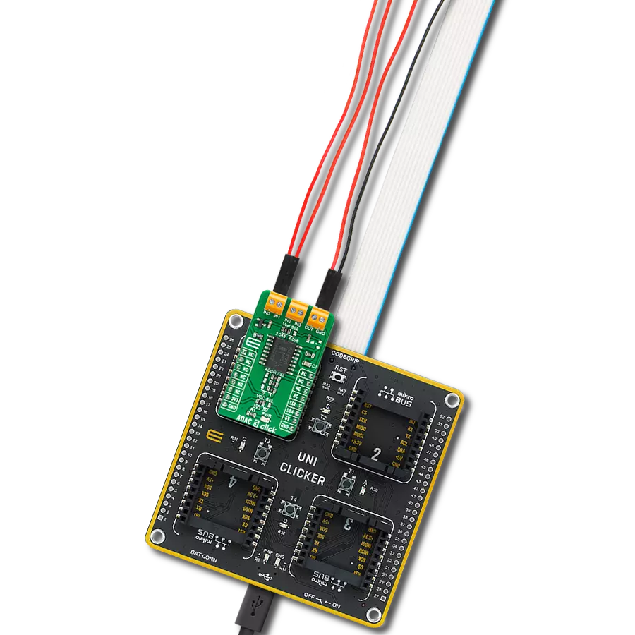
ADAC 3 Click
Dev. board
UNI Clicker
Compiler
NECTO Studio
MCU
TM4C129ENCPDT
High-performance data acquisition solution
A
A
Hardware Overview
How does it work?
ADAC 3 Click is based on the PCF8591, a low-power CMOS data acquisition device from NXP Semiconductors. The PCF8591 comes with four analog inputs configurable as single-ended or differential inputs used to measure voltages, alongside one analog output representing an 8-bit digital-to-analog converter. In addition to measuring voltage, the user can create them as desired and even use DAC and ADC together to generate an input to a circuit and measure the results with the ADC, making it suitable for various control, monitoring, or measurement applications. By its internal structure, the PCF8591 also consists of
an analog input multiplexing circuit and an on-chip track and hold function alongside a serial interface block. This Click board™ communicates with MCU using the standard I2C 2-Wire interface with a maximum clock frequency of 100kHz. The PCF8591 has a 7-bit slave address with the first four MSBs fixed to 1001. The address pins A0, A1, and A2 are programmed by the user and determine the value of the last three LSBs of the slave address, which can be selected by positioning onboard SMD jumpers labeled as ADDR SEL to an appropriate position marked as 0 or 1. Besides, the user can choose the PCF8591
reference voltage value by positioning the SMD jumper labeled VREF SEL, choosing between 2,048 and 4,096V provided by MAX6104 and MAX6106. This Click board™ can operate with either 3.3V or 5V logic voltage levels selected via the VCC SEL jumper. This way, both 3.3V and 5V capable MCUs can use the communication lines properly. However, the Click board™ comes equipped with a library containing easy-to-use functions and an example code that can be used, as a reference, for further development.

Features overview
Development board
UNI Clicker is a compact development board designed as a complete solution that brings the flexibility of add-on Click boards™ to your favorite microcontroller, making it a perfect starter kit for implementing your ideas. It supports a wide range of microcontrollers, such as different ARM, PIC32, dsPIC, PIC, and AVR from various vendors like Microchip, ST, NXP, and TI (regardless of their number of pins), four mikroBUS™ sockets for Click board™ connectivity, a USB connector, LED indicators, buttons, a debugger/programmer connector, and two 26-pin headers for interfacing with external electronics. Thanks to innovative manufacturing technology, it allows you to build
gadgets with unique functionalities and features quickly. Each part of the UNI Clicker development kit contains the components necessary for the most efficient operation of the same board. In addition to the possibility of choosing the UNI Clicker programming method, using a third-party programmer or CODEGRIP/mikroProg connected to onboard JTAG/SWD header, the UNI Clicker board also includes a clean and regulated power supply module for the development kit. It provides two ways of board-powering; through the USB Type-C (USB-C) connector, where onboard voltage regulators provide the appropriate voltage levels to each component on the board, or using a Li-Po/Li
Ion battery via an onboard battery connector. All communication methods that mikroBUS™ itself supports are on this board (plus USB HOST/DEVICE), including the well-established mikroBUS™ socket, a standardized socket for the MCU card (SiBRAIN standard), and several user-configurable buttons and LED indicators. UNI Clicker is an integral part of the Mikroe ecosystem, allowing you to create a new application in minutes. Natively supported by Mikroe software tools, it covers many aspects of prototyping thanks to a considerable number of different Click boards™ (over a thousand boards), the number of which is growing every day.

Microcontroller Overview
MCU Card / MCU
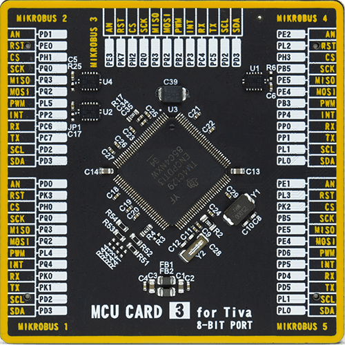
Type
8th Generation
Architecture
ARM Cortex-M4
MCU Memory (KB)
1024
Silicon Vendor
Texas Instruments
Pin count
128
RAM (Bytes)
262144
Used MCU Pins
mikroBUS™ mapper
Take a closer look
Click board™ Schematic

Step by step
Project assembly

Start by selecting your development board and Click board™. Begin with the UNI Clicker as your development board.


Track your results in real time
Application Output
1. Application Output - In Debug mode, the 'Application Output' window enables real-time data monitoring, offering direct insight into execution results. Ensure proper data display by configuring the environment correctly using the provided tutorial.

2. UART Terminal - Use the UART Terminal to monitor data transmission via a USB to UART converter, allowing direct communication between the Click board™ and your development system. Configure the baud rate and other serial settings according to your project's requirements to ensure proper functionality. For step-by-step setup instructions, refer to the provided tutorial.

3. Plot Output - The Plot feature offers a powerful way to visualize real-time sensor data, enabling trend analysis, debugging, and comparison of multiple data points. To set it up correctly, follow the provided tutorial, which includes a step-by-step example of using the Plot feature to display Click board™ readings. To use the Plot feature in your code, use the function: plot(*insert_graph_name*, variable_name);. This is a general format, and it is up to the user to replace 'insert_graph_name' with the actual graph name and 'variable_name' with the parameter to be displayed.

Software Support
Library Description
This library contains API for ADAC 3 Click driver.
Key functions:
adac3_write_controlThis function writes a control byte by using I2C serial interface.adac3_write_dacThis function writes a DAC byte by using I2C serial interface.adac3_read_adcThis function reads the AD conversion byte by using I2C serial interface.
Open Source
Code example
The complete application code and a ready-to-use project are available through the NECTO Studio Package Manager for direct installation in the NECTO Studio. The application code can also be found on the MIKROE GitHub account.
/*!
 * @file main.c
 * @brief ADAC3 Click example
 *
 * # Description
 * This example demonstrates the use of ADAC 3 Click board by setting the DAC output
 * and reading the ADC results from 2 single-ended channels (AIN0, AIN1) and from a
 * differential channel (AIN2+, AIN3-).
 *
 * The demo application is composed of two sections :
 *
 * ## Application Init
 * Initializes the driver and performs the Click default configuration which enables
 * DAC output, sets the analog input mode to single-ended (AIN0, AIN1) and
 * differential (AIN2+, AIN3-), and enables the auto increment mode.
 *
 * ## Application Task
 * Sets the DAC output increasing the value by 1 after each iteration, and reads the
 * ADC results from 2 single-ended and 1 differential channels, and displays the results
 * on the USB UART every 100ms approximately.
 *
 * @note
 * Inputs should be connected to GND when not in use.
 *
 * @author Stefan Filipovic
 *
 */

#include "board.h"
#include "log.h"
#include "adac3.h"

static adac3_t adac3;
static log_t logger;

void application_init ( void )
{
    log_cfg_t log_cfg;  /**< Logger config object. */
    adac3_cfg_t adac3_cfg;  /**< Click config object. */

    /**
     * Logger initialization.
     * Default baud rate: 115200
     * Default log level: LOG_LEVEL_DEBUG
     * @note If USB_UART_RX and USB_UART_TX
     * are defined as HAL_PIN_NC, you will
     * need to define them manually for log to work.
     * See @b LOG_MAP_USB_UART macro definition for detailed explanation.
     */
    LOG_MAP_USB_UART( log_cfg );
    log_init( &logger, &log_cfg );
    log_info( &logger, " Application Init " );

    // Click initialization.
    adac3_cfg_setup( &adac3_cfg );
    ADAC3_MAP_MIKROBUS( adac3_cfg, MIKROBUS_1 );
    if ( I2C_MASTER_ERROR == adac3_init( &adac3, &adac3_cfg ) )
    {
        log_error( &logger, " Communication init." );
        for ( ; ; );
    }

    if ( ADAC3_ERROR == adac3_default_cfg ( &adac3 ) )
    {
        log_error( &logger, " Default configuration." );
        for ( ; ; );
    }

    log_info( &logger, " Application Task " );
}

void application_task ( void )
{
    static uint8_t dac = 0;
    uint8_t ain0, ain1, ain2_ain3_diff;
    if ( ADAC3_OK == adac3_write_dac ( &adac3, dac ) )
    {
        log_printf ( &logger, " DAC : %u mV\r\n",
                     ( uint16_t ) ( ( ADAC3_VREF_2048mV / ADAC3_RESOLUTION ) * dac++ ) );
    }
    if ( ADAC3_OK == adac3_read_adc ( &adac3, &ain0 ) )
    {
        log_printf ( &logger, " AIN0+: %u mV\r\n",
                     ( uint16_t ) ( ( ADAC3_VREF_2048mV / ADAC3_RESOLUTION ) * ain0 ) );
    }
    if ( ADAC3_OK == adac3_read_adc ( &adac3, &ain1 ) )
    {
        log_printf ( &logger, " AIN1+: %u mV\r\n",
                     ( uint16_t ) ( ( ADAC3_VREF_2048mV / ADAC3_RESOLUTION ) * ain1 ) );
    }
    if ( ADAC3_OK == adac3_read_adc ( &adac3, &ain2_ain3_diff ) )
    {
        log_printf ( &logger, " AIN2+ - AIN3-: %d mV\r\n\n",
                     ( int16_t ) ( ( ADAC3_VREF_2048mV / ADAC3_RESOLUTION ) * ( int8_t ) ain2_ain3_diff ) );
    }
    Delay_ms ( 100 );
}

int main ( void )
{
    /* Do not remove this line or clock might not be set correctly. */
    #ifdef PREINIT_SUPPORTED
    preinit();
    #endif

    application_init( );

    for ( ; ; )
    {
        application_task( );
    }

    return 0;
}

// ------------------------------------------------------------------------ END


