Change analog signals to digital with MAX22005 and STM32F303RC
Digitize your data
Published Mar 11, 2023
Click board™
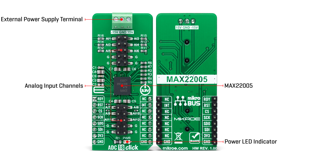
ADC 18 Click
Dev. board
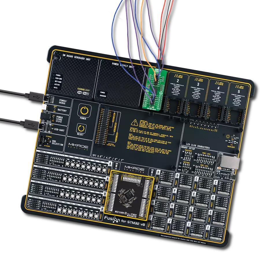
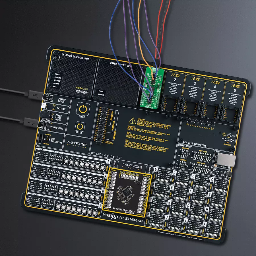
Fusion for STM32 v8
Compiler
NECTO Studio
MCU
STM32F303RC
Translate analog signals for data processing purposes
A
A
Hardware Overview
How does it work?
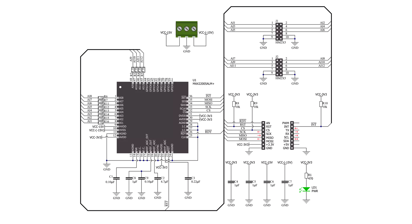
ADC 18 Click is based on the MAX22005, a high-performance twelve-channel analog-to-digital converter from Analog Devices. The MAX22005 has an integrated 24-bit delta-sigma ADC, input multiplexer, signal conditioning, and control logic block, allowing ADC to communicate with MCU through a high-speed serial interface. An integrated delta-sigma ADC is shared between all channels with an integrated 5ppm/°C precision reference. Using high-voltage, zero-drift input amplifiers, standard industrial analog input voltage ranges are converted to the ADC input voltage range. Input channels can be used as twelve single-ended, six differential, and up to eight multichannel configurable differential inputs. In total, the device supports up to 26 different configurations. The MAX22005 can also be configured as an analog-input
current-mode device using an external precision resistor per channel or configurable analog input using an external precision resistor and low-cost switch per channel. All input ports are robustly protected up to ±36V reverse polarity and ±2kV surge pulses without the need for TVS diodes and factory calibrated with a best-in-class system performance of less than 0.05% FSR Total-Unadjusted-Error (TUE) over temperature. ADC 18 Click communicates with MCU through a standard SPI interface and operates at clock rates up to 30MHz, for all configurations and information management and acquiring conversion results. In addition, it also uses several mikroBUS™ pins. An active-low reset signal routed on the RST pin of the mikroBUS™ socket activates a hardware reset of the system, while the INT pin on the mikroBUS™
socket represents a standard interrupt feature providing a user with feedback information. It also has an additional data-ready interrupt marked as RDY and routed on the AN pin of the mikroBUS™ socket, used to signal when a new ADC conversion result is available in the data register. This Click board™ can only be operated with a 3.3V logic voltage level. It also has an analog inputs external power supply terminal where it is necessary to bring ±15V to accept ± 10V inputs, whose full-scale range is ± 12.5V. The board must perform appropriate logic voltage level conversion before using MCUs with different logic levels. However, the Click board™ comes equipped with a library containing functions and an example code that can be used, as a reference, for further development.
Features overview
Development board
Fusion for STM32 v8 is a development board specially designed for the needs of rapid development of embedded applications. It supports a wide range of microcontrollers, such as different 32-bit ARM® Cortex®-M based MCUs from STMicroelectronics, regardless of their number of pins, and a broad set of unique functions, such as the first-ever embedded debugger/programmer over WiFi. The development board is well organized and designed so that the end-user has all the necessary elements, such as switches, buttons, indicators, connectors, and others, in one place. Thanks to innovative manufacturing technology, Fusion for STM32 v8 provides a fluid and immersive working experience, allowing
access anywhere and under any circumstances at any time. Each part of the Fusion for STM32 v8 development board contains the components necessary for the most efficient operation of the same board. An advanced integrated CODEGRIP programmer/debugger module offers many valuable programming/debugging options, including support for JTAG, SWD, and SWO Trace (Single Wire Output)), and seamless integration with the Mikroe software environment. Besides, it also includes a clean and regulated power supply module for the development board. It can use a wide range of external power sources, including a battery, an external 12V power supply, and a power source via the USB Type-C (USB-C) connector.
Communication options such as USB-UART, USB HOST/DEVICE, CAN (on the MCU card, if supported), and Ethernet is also included. In addition, it also has the well-established mikroBUS™ standard, a standardized socket for the MCU card (SiBRAIN standard), and two display options for the TFT board line of products and character-based LCD. Fusion for STM32 v8 is an integral part of the Mikroe ecosystem for rapid development. Natively supported by Mikroe software tools, it covers many aspects of prototyping and development thanks to a considerable number of different Click boards™ (over a thousand boards), the number of which is growing every day.

Microcontroller Overview
MCU Card / MCU
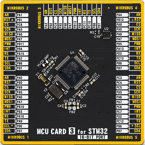
Type
8th Generation
Architecture
ARM Cortex-M4
MCU Memory (KB)
256
Silicon Vendor
STMicroelectronics
Pin count
64
RAM (Bytes)
49152
Used MCU Pins
mikroBUS™ mapper
Take a closer look
Click board™ Schematic
Step by step
Project assembly

Start by selecting your development board and Click board™. Begin with the Fusion for STM32 v8 as your development board.


Software Support
Library Description
This library contains API for ADC 18 Click driver.
Key functions:
adc18_set_active_channelThis function sets the active channel.adc18_start_conversionThis function starts the conversion with the selected data rate.adc18_read_voltageThis function reads RAW ADC value of previous conversion and converts it to voltage.
Open Source
Code example
The complete application code and a ready-to-use project are available through the NECTO Studio Package Manager for direct installation in the NECTO Studio. The application code can also be found on the MIKROE GitHub account.
/*!
 * @file main.c
 * @brief ADC18 Click example
 *
 * # Description
 * This example demonstrates the use of ADC 18 Click board by reading
 * the voltage from 12 analog input single-ended channels.
 *
 * The demo application is composed of two sections :
 *
 * ## Application Init
 * Initializes the driver and logger, and performs the Click default configuration.
 *
 * ## Application Task
 * Reads and displays the voltage from 12 analog input single-ended channels
 * on the USB UART approximately once per second.
 *
 * @author Stefan Filipovic
 *
 */

#include "board.h"
#include "log.h"
#include "adc18.h"

static adc18_t adc18;
static log_t logger;

void application_init ( void )
{
    log_cfg_t log_cfg;  /**< Logger config object. */
    adc18_cfg_t adc18_cfg;  /**< Click config object. */

    /**
     * Logger initialization.
     * Default baud rate: 115200
     * Default log level: LOG_LEVEL_DEBUG
     * @note If USB_UART_RX and USB_UART_TX
     * are defined as HAL_PIN_NC, you will
     * need to define them manually for log to work.
     * See @b LOG_MAP_USB_UART macro definition for detailed explanation.
     */
    LOG_MAP_USB_UART( log_cfg );
    log_init( &logger, &log_cfg );
    log_info( &logger, " Application Init " );

    // Click initialization.
    adc18_cfg_setup( &adc18_cfg );
    ADC18_MAP_MIKROBUS( adc18_cfg, MIKROBUS_1 );
    if ( SPI_MASTER_ERROR == adc18_init( &adc18, &adc18_cfg ) )
    {
        log_error( &logger, " Communication init." );
        for ( ; ; );
    }

    if ( ADC18_ERROR == adc18_default_cfg ( &adc18 ) )
    {
        log_error( &logger, " Default configuration." );
        for ( ; ; );
    }

    log_info( &logger, " Application Task " );
}

void application_task ( void )
{
    static uint8_t channel = ADC18_CH_AI1_SINGLE_ENDED;
    if ( ADC18_OK == adc18_set_active_channel ( &adc18, channel ) )
    {
        adc18_start_conversion ( &adc18, ADC18_DATA_RATE_225_SPS );

        // Waits for the availability of the conversion result
        while ( adc18_get_rdy_pin ( &adc18 ) );

        adc18_stop_conversion ( &adc18 );

        float voltage;
        if ( ADC18_OK == adc18_read_voltage ( &adc18, &voltage ) )
        {
            log_printf ( &logger, "Channel AI%u: %.2f V\r\n", channel + 1, voltage );
            if ( ++channel > ADC18_CH_AI12_SINGLE_ENDED )
            {
                channel = ADC18_CH_AI1_SINGLE_ENDED;
                log_printf ( &logger, "\r\n" );
                Delay_ms ( 1000 );
            }
        }
    }
}

int main ( void )
{
    /* Do not remove this line or clock might not be set correctly. */
    #ifdef PREINIT_SUPPORTED
    preinit();
    #endif

    application_init( );

    for ( ; ; )
    {
        application_task( );
    }

    return 0;
}

// ------------------------------------------------------------------------ END


