使用IDC10头和MK64FN1M0VDC12简化其他附加组件与mikroBUS™插座的连接
让兼容性不再是问题!

已发布 6月 24, 2024
点击板
Adapter Click
开发板
Clicker 2 for Kinetis
编译器
NECTO Studio
微控制器单元
MK64FN1M0VDC12
毫不费力地将传感器、驱动程序和其他组件集成到您的项目设置中。
A
A
硬件概览
它是如何工作的?
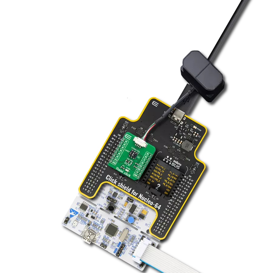
Adapter Click是一个适配器板,简化了将具有IDC10头部的附加组件连接到mikroBUS™插座的过程。一个2x5位置、2.54mm间距的连接器头部允许您以符合项目需求的方式添加传感器、驱动程序和各种组件。每个头部引脚对应于mikroBUS™插座上的一个引脚(除了AN和RST引脚)。多亏了这些引脚,与Click板™的连接始终牢固稳定,始终保持完美的连接质量。建立 这种连接有两种方式:男性或女性IDC10连接器。两
者都包含在包装中。您可以将男性IDC10连接器焊接在Adapter Click的顶部,并直接连接附加板或通过IDC10平线电缆连接。在某些情况下,女性头部插座可能是更好的选择。根据实际情况的方便程度,将其焊接在顶部或底部。Adapter Click允许使用I2C和SPI接口,其中每个mikroBUS™线都覆盖,除了如前所述 的AN和RST线。可以通过将标记为INTERFACE SELECTION的跳线放置在标记为SPI或I2C的适当位
置来进行选择。请注意,所有跳线的位置必须在同一侧,否则Click板™可能会失去响应。这个Click板™可以通过PWR SEL跳线选择3.3V和5V逻辑电压电平。这样,既支持3.3V又支持5V的MCU可以正确地使用通信线路。此外,这个Click板™配备了一个包含易于使用的函数和示例代码的库,可用作进一步开发的参考。

功能概述
开发板
Clicker 2 for Kinetis 是一款紧凑型入门开发板,它将 Click 板™的灵活性带给您喜爱的微控制器,使其成为实现您想法的完美入门套件。它配备了一款板载 32 位 ARM Cortex-M4F 微控制器,NXP 半导体公司的 MK64FN1M0VDC12,两个 mikroBUS™ 插槽用于 Click 板™连接,一个 USB 连接器,LED 指示灯,按钮,一个 JTAG 程序员连接器以及两个 26 针头用于与外部电子设备的接口。其紧凑的设计和清晰、易识别的丝网标记让您能够迅速构建具有独特功能和特性
的小工具。Clicker 2 for Kinetis 开发套件的每个部分 都包含了使同一板块运行最高效的必要组件。除了可以选择 Clicker 2 for Kinetis 的编程方式,使用 USB HID mikroBootloader 或外部 mikroProg 连接器进行 Kinetis 编程外,Clicker 2 板还包括一个干净且调节过的开发套件电源供应模块。它提供了两种供电方式;通过 USB Micro-B 电缆,其中板载电压调节器为板上每个组件提供适当的电压水平,或使用锂聚合物 电池通过板载电池连接器供电。所有 mikroBUS™ 本
身支持的通信方法都在这块板上,包括已经建立良好的 mikroBUS™ 插槽、重置按钮和几个用户可配置的按钮及 LED 指示灯。Clicker 2 for Kinetis 是 Mikroe 生态系统的一个组成部分,允许您在几分钟内创建新的应用程序。它由 Mikroe 软件工具原生支持,得益于大量不同的 Click 板™(超过一千块板),其数量每天都在增长,它涵盖了原型制作的许多方面。

微控制器概述
MCU卡片 / MCU

建筑
ARM Cortex-M4
MCU 内存 (KB)
1024
硅供应商
NXP
引脚数
121
RAM (字节)
262144
使用的MCU引脚
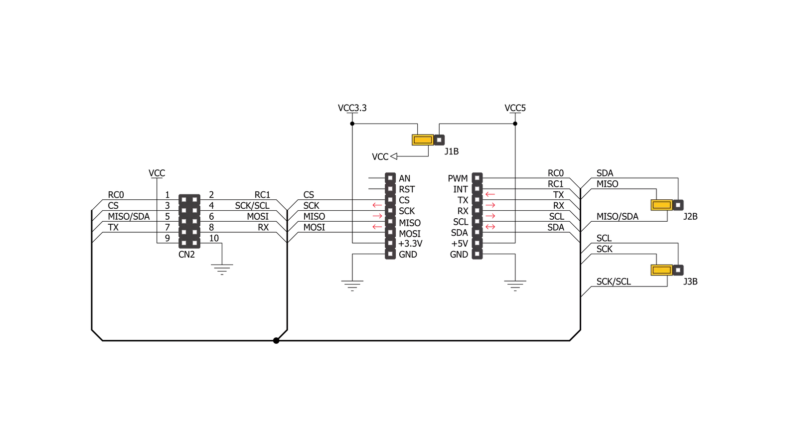
mikroBUS™映射器
“仔细看看!”
Click board™ 原理图
一步一步来
项目组装

从选择您的开发板和Click板™开始。以Clicker 2 for Kinetis作为您的开发板开始。


实时跟踪您的结果
应用程序输出
1. 应用程序输出 - 在调试模式下,“应用程序输出”窗口支持实时数据监控,直接提供执行结果的可视化。请按照提供的教程正确配置环境,以确保数据正确显示。

2. UART 终端 - 使用UART Terminal通过USB to UART converter监视数据传输,实现Click board™与开发系统之间的直接通信。请根据项目需求配置波特率和其他串行设置,以确保正常运行。有关分步设置说明,请参考提供的教程。

3. Plot 输出 - Plot功能提供了一种强大的方式来可视化实时传感器数据,使趋势分析、调试和多个数据点的对比变得更加直观。要正确设置,请按照提供的教程,其中包含使用Plot功能显示Click board™读数的分步示例。在代码中使用Plot功能时,请使用以下函数:plot(insert_graph_name, variable_name);。这是一个通用格式,用户需要将“insert_graph_name”替换为实际图表名称,并将“variable_name”替换为要显示的参数。

软件支持
库描述
这个库包含Adapter Click驱动程序的API。
关键功能:
adapter_generic_write- 将数据写入到指定的寄存器。adapter_generic_read- 从指定的寄存器读取数据。
开源
代码示例
完整的应用程序代码和一个现成的项目可以通过NECTO Studio包管理器直接安装到NECTO Studio。 应用程序代码也可以在MIKROE的GitHub账户中找到。
/*!
 * \file
 * \brief Adapter Click example
 *
 * # Description
 * Adapter Click is a breakout board which simplifies connection of add-on boards.
 * There are two ways of establishing connection: using male or female IDC10 connectors.
 * Male header must be soldered on the top side of Adapter Click to connect the add-on board
 * directly or via flat cable. Female header can be soldered either on the top, or the bottom
 * side, depending on which one is more convenient in given circumstances.
 * There are two jumpers for SPI/I2C selection and one for selection of power supply range.
 *
 * The demo application is composed of two sections :
 *
 * ## Application Init
 * Initalizes I2C or SPI driver and makes an initial log.
 *
 * ## Application Task
 * This is an example that shows the use of the Adapter Click board (SPI mode -  set as default).
 * In I2C mode we are reading internal temperature from another device (THERMO 5 Click board).
 * In SPI mode example we are writing "mikroElektronika" to SRAM Click board,
 * and then reading from the same memory location.
 *
 * ## Additional Functions
 *   - float thermo5_read_inter_temp ( adapter_t *ctx ) -
 *     @description Function reads measurements made by internal diode.
 *   - void sram_write_byte ( adapter_t *ctx, uint32_t reg_address, uint8_t write_data ) -
 *     @description Function writes the 8-bit data to the target 24-bit register address of 23LC1024 chip.
 *   - uint8_t sram_read_byte ( adapter_t *ctx, uint32_t reg_address ) -
 *     @description Function reads the 8-bit data to the target 24-bit register address of 23LC1024 chip.
 *
 * \author MikroE Team
 *
 */
// ------------------------------------------------------------------- INCLUDES

#include "board.h"
#include "log.h"
#include "adapter.h"

#define THERMO5_INTER_DIO_DATA_HI_BYTE          0x00
#define THERMO5_INTER_DIO_DATA_LO_BYTE          0x29

#define SRAM_24BIT_DATA                         0x00FFFFFF
#define SRAM_CMD_WRITE                          0x02
#define SRAM_CMD_READ                           0x03

// ------------------------------------------------------------------ VARIABLES

static adapter_t adapter;
static log_t logger;

char send_buffer[ 17 ] = { 'm', 'i', 'k', 'r', 'o', 'E', 'l', 'e', 'k', 't', 'r', 'o', 'n', 'i', 'k', 'a', ' ' };
char mem_data[ 17 ];
uint8_t n_cnt;

// ------------------------------------------------------ ADDITIONAL FUNCTIONS

float thermo5_read_inter_temp ( adapter_t *ctx )
{
    uint16_t inter_temp;
    uint8_t high_byte;
    uint8_t low_byte;
    float output;
    output = 0.0;

    adapter_generic_read ( ctx, THERMO5_INTER_DIO_DATA_HI_BYTE, &high_byte, 1 );
    adapter_generic_read ( ctx, THERMO5_INTER_DIO_DATA_LO_BYTE, &low_byte, 1 );

    inter_temp = high_byte;
    inter_temp <<= 8;
    inter_temp |= low_byte;
    inter_temp >>= 5;
    output = ( float )inter_temp;
    output *= 0.125;

    return output;
}

void sram_write_byte ( adapter_t *ctx, uint32_t reg_address, uint8_t write_data )
{
    uint8_t tx_buf[ 4 ];
    uint8_t rx_buf;

    reg_address &= SRAM_24BIT_DATA;

    tx_buf[ 0 ]  = ( uint8_t ) ( reg_address >> 16 );
    tx_buf[ 1 ]  = ( uint8_t ) ( reg_address >> 8 );
    tx_buf[ 2 ]  = ( uint8_t )   reg_address;
    tx_buf[ 3 ]  = write_data;

    adapter_generic_write( ctx, SRAM_CMD_WRITE, tx_buf, 4 );
}

uint8_t sram_read_byte ( adapter_t *ctx, uint32_t reg_address )
{
    uint8_t tx_buf[ 5 ];
    uint8_t rx_buf[ 5 ];
    uint8_t read_data;

    reg_address &= SRAM_24BIT_DATA;

    tx_buf[ 0 ] = SRAM_CMD_READ;
    tx_buf[ 1 ] = ( uint8_t ) ( reg_address >> 16 );
    tx_buf[ 2 ] = ( uint8_t ) ( reg_address >> 8 );
    tx_buf[ 3 ] = ( uint8_t )   reg_address;

    adapter_generic_transfer( ctx, tx_buf, 4, rx_buf, 1 );

    read_data = rx_buf[ 0 ];

    return read_data;
}

// ------------------------------------------------------ APPLICATION FUNCTIONS

void application_init ( void )
{
    log_cfg_t log_cfg;
    adapter_cfg_t cfg;

    /**
     * Logger initialization.
     * Default baud rate: 115200
     * Default log level: LOG_LEVEL_DEBUG
     * @note If USB_UART_RX and USB_UART_TX
     * are defined as HAL_PIN_NC, you will
     * need to define them manually for log to work.
     * See @b LOG_MAP_USB_UART macro definition for detailed explanation.
     */
    LOG_MAP_USB_UART( log_cfg );
    log_init( &logger, &log_cfg );
    log_info( &logger, "---- Application Init ----" );

    //  Click initialization.

    adapter_cfg_setup( &cfg );
    ADAPTER_MAP_MIKROBUS( cfg, MIKROBUS_1 );
    adapter_init( &adapter, &cfg );
}

void application_task ( void )
{
    float temp_value;

    if ( adapter.master_sel == ADAPTER_MASTER_SPI )
    {
        log_printf( &logger, " Writing text :\r\n" );

        for ( n_cnt = 0; n_cnt < 16; n_cnt++ )
        {
            sram_write_byte( &adapter, n_cnt, send_buffer[ n_cnt ] );
            Delay_ms ( 100 );
            log_printf( &logger, "%c", send_buffer[ n_cnt ] );
        }


        log_printf( &logger, "\r\n" );
        log_printf( &logger, " Read text :\r\n" );
        for ( n_cnt = 0; n_cnt < 16; n_cnt++ )
        {
            mem_data[ n_cnt ] = sram_read_byte( &adapter, n_cnt );
            Delay_ms ( 100 );
            log_printf( &logger, "%c", mem_data[ n_cnt ] );
        }
        log_printf( &logger, "\r\n" );
        log_printf( &logger, "--------------------------\r\n" );

        Delay_ms ( 1000 );
    }
    else if ( adapter.master_sel == ADAPTER_MASTER_I2C )
    {
        temp_value = thermo5_read_inter_temp( &adapter );

        log_printf( &logger, " Thermo 5 internal temperature :  %.2f\r\n", temp_value );
        log_printf( &logger, "--------------------------\r\n" );

        Delay_ms ( 1000 );
        Delay_ms ( 1000 );
    }
}

int main ( void )
{
    /* Do not remove this line or clock might not be set correctly. */
    #ifdef PREINIT_SUPPORTED
    preinit();
    #endif

    application_init( );

    for ( ; ; )
    {
        application_task( );
    }

    return 0;
}


// ------------------------------------------------------------------------ END